Samsung patents chip inspection method using multi-wavelength light
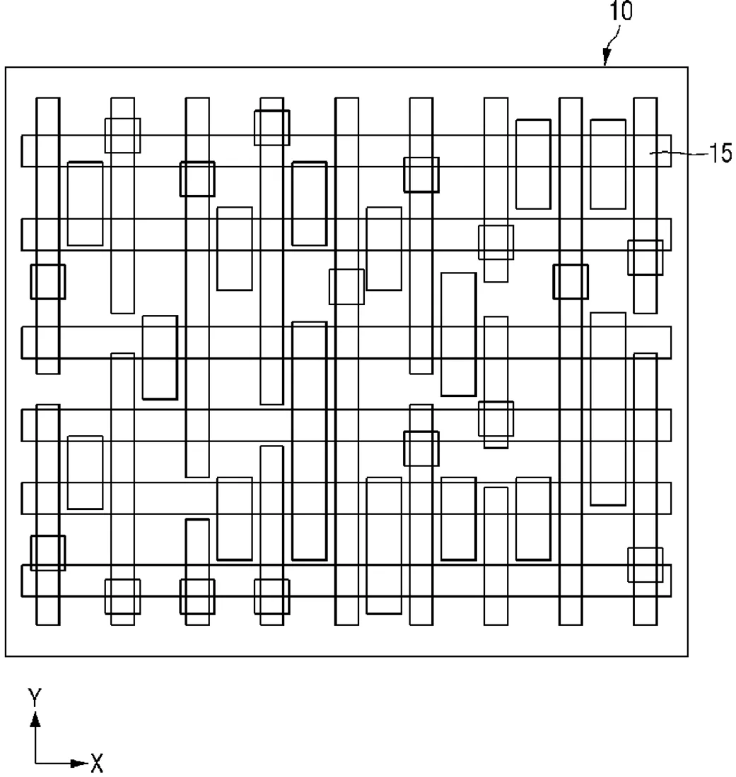
Samsung has been granted a patent for a method to inspect semiconductor wafers by shining light of different colors (wavelengths) onto identical chips. The system compares the light reflected from specific spots on each chip to identify outliers that indicate manufacturing defects.
In the filing’s own words
A method for fabricating a semiconductor device is provided. The method for fabricating the semiconductor device includes a first step of loading a first wafer including a plurality of semiconductor chips having the same pattern on a stage of a wafer inspection apparatus, a second step of inspecting the plurality of semiconductor chips using light having different wavelengths from each other, and a third step of unloading the first wafer from the stage of the wafer inspection apparatus, wherein inspecting of the plurality of semiconductor chips using the light includes inspecting patterns at the same first positions of the respective semiconductor chips, inspecting patterns at the same second positions of the respective semiconductor chips, inspecting patterns at the same k-th positions of the respective semiconductor chips, and determining the semiconductor chip having a pattern defect by combining pattern inspection results at each of the first to k-th positions.
What exactly they claim (claim 1)
1. A method for fabricating a semiconductor device, the method comprising: a first step of loading a first wafer including a plurality of semiconductor chips, each having an identical pattern, on a stage of a wafer inspection apparatus; a second step of inspecting the plurality of semiconductor chips using multiple wavelengths of light; and a third step of unloading the first wafer from the stage of the wafer inspection apparatus, wherein inspecting the plurality of semiconductor chips using the light includes: inspecting patterns at identical first positions of each of the respective semiconductor chips, inspecting patterns at identical second positions of each of the respective semiconductor chips, inspecting patterns at identical k-th positions of each of the respective semiconductor chips, and determining a semiconductor chip of the plurality of semiconductor chips having a pattern defect by combining pattern inspection results for each of the first to k-th positions, k being a natural number of 3 or more, and wherein inspecting the patterns at the identical first positions includes: obtaining a first plurality of pieces of spectral information at the first positions using the multiple wavelengths of light, obtaining a first spectral distribution information from the first plurality of pieces of spectral information, calculating a statistical distribution region from the first spectral distribution information, identifying outlier pieces of spectral information not included in the statistical distribution region among the first plurality of pieces of spectral information, and determining the semiconductor chip having a pattern defect by associating the outlier pieces of spectral information not included in the statistical distribution region as a defect.
Facts
- Company
- Samsung (Samsung Electronics Co., Ltd.)
- Official title
- Method for fabricating a semiconductor device using a wafer inspection apparatus
- Patent number
- US12757687B2
- Application number
- 18382998
- Filed
- Oct 23, 2023
- Granted
- Oct 6, 2026
- Inventors
- 5
- Claims
- 20
Classified under
H10P 74/203 Electricity & electronicsG01N 21/9501 Physics & computingMore from Samsung in Chips & hardware
- Samsung patents chip that combines camera and screen Oct 13, 2026
- Samsung patents faster chip testing using machine learning Sep 1, 2026
- Samsung patents radar method to pinpoint target direction more accurately Sep 1, 2026
- Samsung patents memory chip that searches data by content, not address Sep 1, 2026
- Samsung patents chip design that skips empty data to speed up AI Sep 1, 2026
Summaries are simplified from the filing’s own abstract and first claim. A patent filing is not a product announcement.
Patent data and drawings: U.S. Patent and Trademark Office (USPTO). Nebula is not affiliated with or endorsed by the USPTO.