Samsung patents display panel that combines screen and light sensor
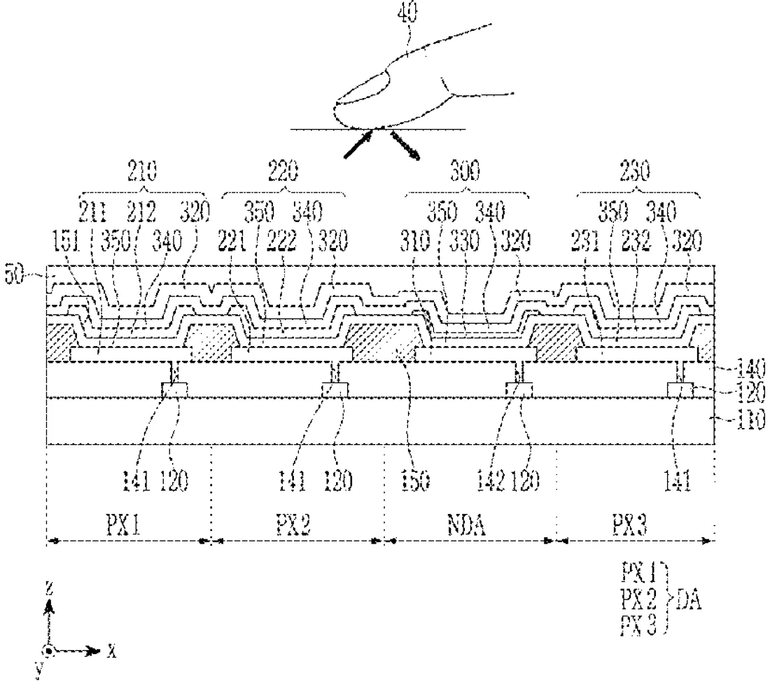
Samsung describes a display panel where the light-emitting pixels and light-detecting sensors share the same underlying material layers. This design allows the sensor to sit directly next to the screen components, potentially making the device thinner and simpler to build.
In the filing’s own words
A sensor-embedded display panel includes a light emitting element on a substrate and including a light emitting layer, and a photosensor on the substrate and including a photosensitive layer extending at least partially in parallel with the light emitting layer along an in-plane direction of the substrate. The light emitting element and the photosensor include separate, respective portions of each of first and second common auxiliary layers each extending continuously as a single piece of material under and on, respectively, each of the light emitting layer and the photosensitive layer. The photosensitive layer may include a light absorbing semiconductor having a HOMO energy level having a difference of less than about 1.0 eV from a HOMO energy level of the first common auxiliary layer and a LUMO energy level having a difference of less than about 1.0 eV from a LUMO energy level of the second common auxiliary layer.
What exactly they claim (claim 1)
1. A sensor-embedded display panel, comprising: a light emitting element on a substrate, the light emitting element including a light emitting layer, and a photosensor on the substrate, the photosensor including a photosensitive layer, the photosensitive layer extending at least partially in parallel with the light emitting layer along an in-plane direction of the substrate, wherein the light emitting element and the photosensor each include a separate portion of a first common auxiliary layer extending continuously as a single first piece of material under each of the light emitting layer and the photosensitive layer; and a separate portion of a second common auxiliary layer extending continuously as a single second piece of material on each of the light emitting layer and the photosensitive layer, wherein the photosensitive layer includes a light absorbing semiconductor having a HOMO energy level having a difference of less than about 1.0 eV from a HOMO energy level of the first common auxiliary layer and a LUMO energy level having a difference of less than about 1.0 eV from a LUMO energy level of the second common auxiliary layer, wherein the photosensitive layer does not include any counterpart semiconductor for any pn junction with the light absorbing semiconductor, wherein the light absorbing semiconductor is an organic light absorbing material, and wherein the organic light absorbing material is represented by at least one of Chemical Formula 1: wherein, in Chemical Formula 1, X is O, S, Se, Te, SO, SO 2, CR b R c, or SiR d R e, Ar is a substituted or unsubstituted C6 to C30 arylene group, a substituted or unsubstituted C3 to C30 heterocyclic group, or fused rings thereof, Ar 1a and Ar 2a are each independently a substituted or unsubstituted C6 to C30 aryl(ene) group or a substituted or unsubstituted C3 to C30 heteroaryl(ene) group, R 1a to R 3a and R b to R e are each independently hydrogen, a substituted or unsubstituted C1 to C30 alkyl group, a substituted or unsubstituted C1 to C30 alkoxy group, a substituted or unsubstituted C6 to C30 aryl group, a substituted or unsubstituted C3 to C30 heteroaryl group, a halogen, a cyano group, or any combination thereof, and Ar 1a, Ar 2a, R 1a, and R 2a are each independently present, or two adjacent ones of Ar 1a, Ar 2a, R 1a, and R 2a are linked to each other to form a ring, and wherein the light emitting layer includes an organic light emitting material, and difference between respective sublimation temperatures of the organic light absorbing material and the organic light emitting material is greater than or equal to about 0° C. and less than about 100° C.
Facts
- Company
- Samsung (Samsung Electronics Co., Ltd.)
- Official title
- Photosensor and sensor embedded display panel and electronic device
- Patent number
- US12757564B2
- Application number
- 18317400
- Filed
- May 15, 2023
- Granted
- Oct 6, 2026
- Inventors
- 9
- Claims
- 15
Classified under
H10K 39/34 Electricity & electronicsH10K 39/501 Electricity & electronicsH10K 59/60 Electricity & electronicsH10K 59/65 Electricity & electronicsH10K 65/00 Electricity & electronicsH10K 50/852 Electricity & electronicsMore from Samsung in Chips & hardware
- Samsung patents chip that combines camera and screen Oct 13, 2026
- Samsung patents faster chip testing using machine learning Sep 1, 2026
- Samsung patents radar method to pinpoint target direction more accurately Sep 1, 2026
- Samsung patents memory chip that searches data by content, not address Sep 1, 2026
- Samsung patents chip design that skips empty data to speed up AI Sep 1, 2026
Summaries are simplified from the filing’s own abstract and first claim. A patent filing is not a product announcement.
Patent data and drawings: U.S. Patent and Trademark Office (USPTO). Nebula is not affiliated with or endorsed by the USPTO.