Samsung patents LED structure that boosts light output with layered films
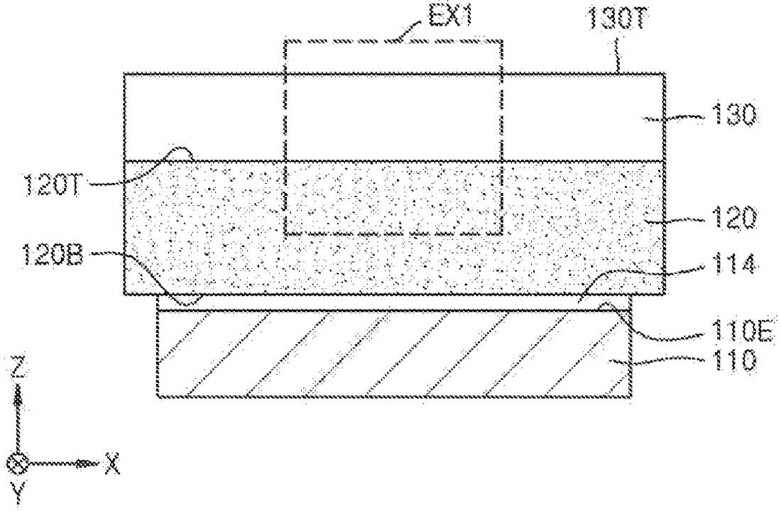
Samsung has been granted a patent for a light-emitting device that uses a semiconductor chip to generate light, which is then shifted to a different color by a conversion layer. Above this setup is a coating made of alternating thin inorganic films designed to let specific wavelengths of light pass through while reflecting others to improve efficiency.
In the filing’s own words
A light-emitting device includes: a semiconductor light-emitting structure configured to emit light having a first wavelength; a wavelength conversion layer configured to convert the light which has the first wavelength into light having a second wavelength that is greater than the first wavelength; and a multi-inorganic-film coating layer spaced apart from a light-emitting surface with the wavelength conversion layer therebetween. The multi-inorganic-film coating layer includes a distributed Bragg reflector structure in which first and second inorganic films are alternately stacked, and an uppermost inorganic film farthest from the wavelength conversion layer from among the plurality of inorganic films has a greatest thickness in a first direction perpendicular to the light-emitting surface of the semiconductor light-emitting structure. The first refractive index is selected from a range of about 1.1 to about 1.5, and the second refractive index is selected from a range of about 2.0 to about 3.0.
What exactly they claim (claim 1)
1. A light-emitting device comprising: a semiconductor light-emitting structure configured to emit light having a first wavelength through a light-emitting surface; a wavelength conversion layer facing the light-emitting surface and configured to convert at least a portion of the light which has the first wavelength into light having a second wavelength that is greater than the first wavelength; and a multi-inorganic-film coating layer spaced apart from the light-emitting surface with the wavelength conversion layer therebetween, the multi-inorganic-film coating layer being configured to simultaneously transmit both a portion of the light having the first wavelength and a portion of the light having the second wavelength, which are incident from the wavelength conversion layer, wherein the multi-inorganic-film coating layer comprises a distributed Bragg reflector (DBR) structure comprising a plurality of inorganic films, in which a first inorganic film having a first refractive index and a second inorganic film having a second refractive index are alternately stacked, and an uppermost inorganic film farthest from the wavelength conversion layer from among the plurality of inorganic films has a greatest thickness in a first direction perpendicular to the light-emitting surface of the semiconductor light-emitting structure, and wherein the first refractive index is selected from a range of about 1.1 to about 1.5 and the second refractive index is selected from a range of about 2.0 to about 3.0.
Facts
- Company
- Samsung (SAMSUNG ELECTRONICS CO., LTD.)
- Official title
- Light-emitting device
- Patent number
- US12757536B2
- Application number
- 18371835
- Filed
- Sep 22, 2023
- Granted
- Oct 6, 2026
- Inventors
- 4
- Claims
- 20
Classified under
H10H 20/841 Electricity & electronicsH10H 20/8512 Electricity & electronicsH10H 29/8421 Electricity & electronicsH10H 29/8512 Electricity & electronicsMore from Samsung in Chips & hardware
- Samsung patents chip that combines camera and screen Oct 13, 2026
- Samsung patents faster chip testing using machine learning Sep 1, 2026
- Samsung patents radar method to pinpoint target direction more accurately Sep 1, 2026
- Samsung patents memory chip that searches data by content, not address Sep 1, 2026
- Samsung patents chip design that skips empty data to speed up AI Sep 1, 2026
Summaries are simplified from the filing’s own abstract and first claim. A patent filing is not a product announcement.
Patent data and drawings: U.S. Patent and Trademark Office (USPTO). Nebula is not affiliated with or endorsed by the USPTO.