Microsoft patents image sensor design that cuts noise by shrinking light-capture areas
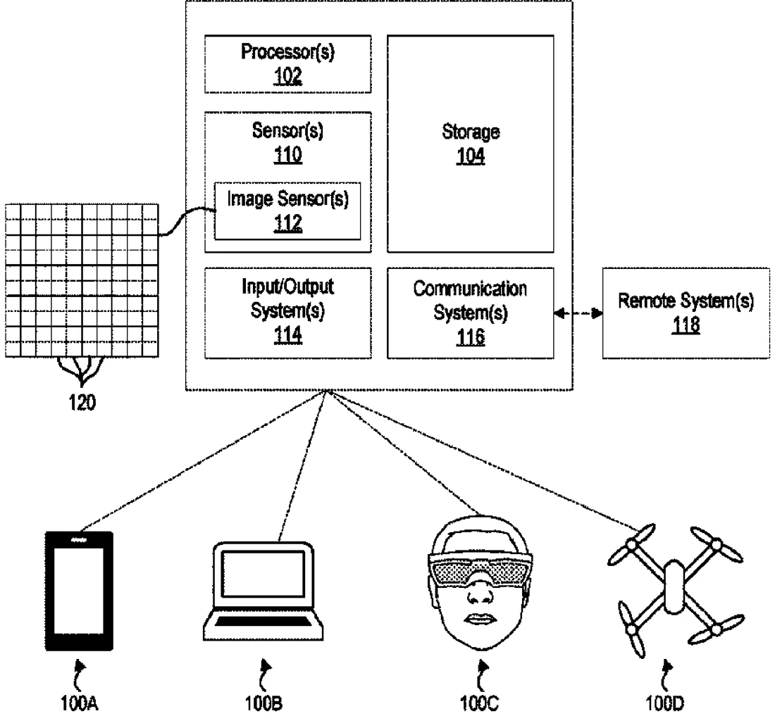
Microsoft describes an image sensor where the light-sensitive part of each pixel is smaller than the space between pixels. This smaller size reduces unwanted electrical noise, while oxide layers separate the pixels to further improve image quality.
In the filing’s own words
An image sensor comprises a plurality of image sensing pixels arranged to form a sensor array. Each image sensing pixel of the plurality of image sensing pixels comprises a semiconductor photodetector connected to a photosensitive region that comprises a photon reception area configured to receive photons to facilitate image capture. For at least a particular image sensing pixel of the plurality of image sensing pixels, the length or the width of the photon reception area is smaller than about 80% of a pixel pitch measurement between the particular image sensing pixel and an adjacent image sensing pixel, which contributes to reduced volume of the photosensitive region and mitigated sensor noise. A space between the photosensitive region of the particular image sensing pixel and the photosensitive region of the adjacent image sensing pixel comprises at least one oxide layer and/or at least one metal layer.
What exactly they claim (claim 1)
1. An image sensor configured to capture imagery with mitigated noise, the image sensor comprising: a plurality of image sensing pixels arranged to form a sensor array, wherein: each image sensing pixel of the plurality of image sensing pixels comprises a semiconductor photodetector connected to a photosensitive region that comprises a photon reception area configured to receive photons to facilitate image capture, each photon reception area comprises a length and a width, for at least a particular image sensing pixel of the plurality of image sensing pixels, the length or the width of the photon reception area is smaller than about 80% of a pixel pitch measurement between the particular image sensing pixel and an adjacent image sensing pixel of the plurality of image sensing pixels, wherein the length or the width of the photon reception area contributes to reduced volume of the photosensitive region to mitigate sensor noise for the image sensor, and a space between the photosensitive region of the particular image sensing pixel and the photosensitive region of the adjacent image sensing pixel comprises a plurality of oxide layers arranged transverse to the photon reception area, wherein the plurality of oxide layers comprises a first oxide layer arranged adjacent to the photosensitive region of the particular image sensing pixel and a second oxide layer arranged adjacent to the photosensitive region of the adjacent image sensing pixel.
Facts
- Company
- Microsoft (Microsoft Technology Licensing, LLC)
- Official title
- Image sensing pixel configurations for reduced dark current noise
- Patent number
- US12757505B2
- Application number
- 18484267
- Filed
- Oct 10, 2023
- Granted
- Oct 6, 2026
- Inventors
- 2
- Claims
- 18
Classified under
H10F 39/8027 Electricity & electronicsH10F 39/18 Electricity & electronicsH10F 39/8023 Electricity & electronicsH10F 39/8063 Electricity & electronicsH10F 39/807 Electricity & electronicsMore from Microsoft in Chips & hardware
- Microsoft patents chips with liquid cooling built inside Oct 1, 2026
- Microsoft patents chip design that guesses code steps ahead Sep 8, 2026
- Microsoft patents 3D glass storage using laser light patterns Sep 8, 2026
- Microsoft patents hand-held radar reflectors for tracking movement Sep 8, 2026
- Microsoft patents video boost that reuses old frames to save power Sep 15, 2026
Summaries are simplified from the filing’s own abstract and first claim. A patent filing is not a product announcement.
Patent data and drawings: U.S. Patent and Trademark Office (USPTO). Nebula is not affiliated with or endorsed by the USPTO.