Samsung patents uneven semiconductor fins to improve chip structure
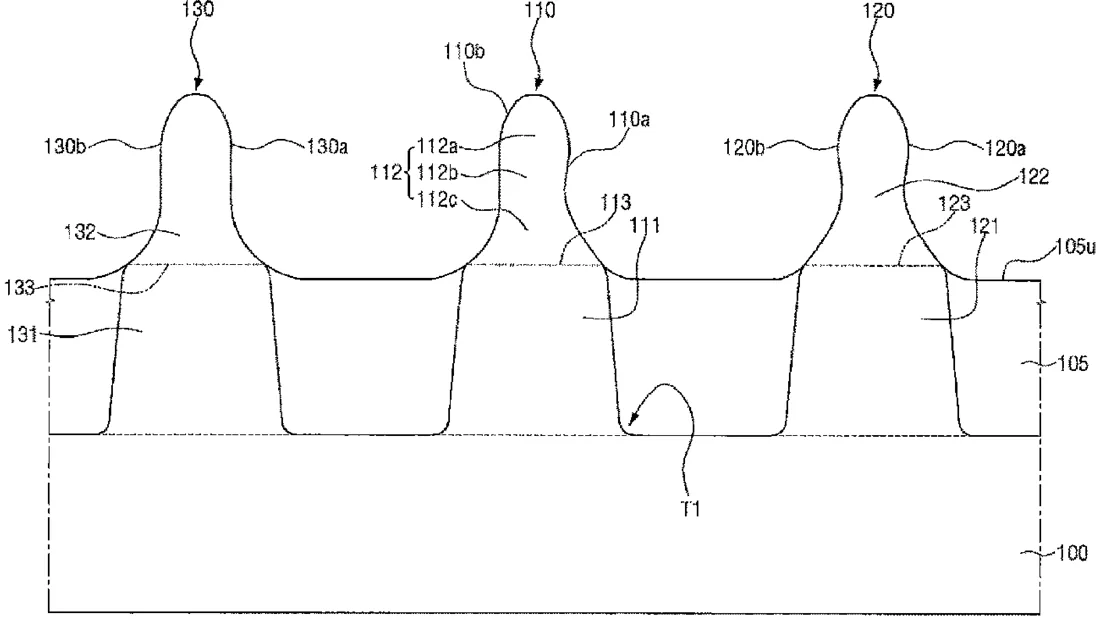
This patent describes a specific shape for the vertical structures, or fins, inside a computer chip. The design features a central fin that is narrower than the two fins on either side, with a wavy side profile that changes width as it rises. This arrangement is intended to optimize the physical layout of the transistor components on the silicon substrate.
In the filing’s own words
A semiconductor device can include a field insulating film on a substrate and a fin-type pattern of a particular material, on the substrate, having a first sidewall and an opposing second sidewall. The fin-type pattern can include a first portion of the fin-type pattern that protrudes from an upper surface of the field insulating film and a second portion of the fin-type pattern disposed on the first portion. A third portion of the fin-type pattern can be disposed on the second portion where the third portion can be capped by a top rounded surface of the fin-type pattern and the first sidewall can have an undulated profile that spans the first, second and third portions.
What exactly they claim (claim 1)
1. A semiconductor device comprising: a substrate; a first fin-type pattern disposed on the substrate, and including a first lower portion and a first protruding portion on the first lower portion; a second fin-type pattern disposed on the substrate, and including a second lower portion and a second protruding portion on the second lower portion; a third fin-type pattern disposed on the substrate, wherein the second fin-type pattern is disposed in a space between the first fin-type pattern and the third fin-type pattern, wherein the first fin-type pattern and the second fin-type pattern are spaced apart from each other at a first distance in a first horizontal direction parallel to an upper surface of the substrate, wherein the first fin-type pattern and the third fin-type pattern are spaced apart from each other at a second distance in the first horizontal direction, and wherein the second distance is different from the first distance; and a field insulating film disposed on the substrate and disposed between the first lower portion of the first fin-type pattern and the second lower portion of the second fin-type pattern, wherein the first protruding portion of the first fin-type pattern protrudes beyond an upper surface of the field insulating film, wherein the first protruding portion includes a first point, a second point at which the first protruding portion has a first width, and a third point at which the first protruding portion has a second width less than the first width of the first protruding portion, wherein the second point of the first protruding portion is higher than the third point of the first protruding portion, and the first point of the first protruding portion is higher than the second point of the first protruding portion, wherein a maximum width of the first protruding portion is a width at a first boundary between the first protruding portion and the first lower portion, wherein a first portion, between the second point and an uppermost end of the first protruding portion, of the first protruding portion is a decreasing width in a vertical direction along which a distance from the upper surface of the substrate increases, wherein a second portion, between the third point and the second point, of the first protruding portion is an increasing width in the vertical direction, wherein a third portion, between the first boundary and the third point, of the first protruding portion has a decreasing width in the vertical direction, wherein the second point of the first protruding portion is at a boundary between the first and second portions of the first protruding portion, and the third point of the first protruding portion is at a boundary between the second and third portions of the first protruding portion, wherein the second protruding portion of the second fin-type pattern protrudes beyond the upper surface of the field insulating film, wherein the second protruding portion includes a first point, a second point at which the second protruding portion has a third width, and a third point at which the second protruding portion has a fourth width less than the third width of the second protruding portion, wherein the second point of the second protruding portion is higher than the third point of the second protruding portion, and the first point of the second protruding portion is higher than the second point of the second protruding portion, wherein a maximum width of the second protruding portion is a width at a second boundary between the second protruding portion and the second lower portion, wherein a first portion, between the second point and an uppermost end of the second protruding portion, of the second protruding portion is a decreasing width in the vertical direction, wherein a second portion, between the third point and the second point, of the second protruding portion is an increasing width in the vertical direction, wherein a third portion, between the second boundary and the third point,
Facts
- Company
- Samsung (SAMSUNG ELECTRONICS CO., LTD.)
- Official title
- Semiconductor device having an asymmetric fin-type patterns formed between two symmetric fin-type patterns with varying width along center vertical line of the fins
- Patent number
- US12757368B2
- Application number
- 18604195
- Filed
- Mar 13, 2024
- Granted
- Oct 6, 2026
- Inventors
- 3
- Claims
- 9
Classified under
H10B 10/12 Electricity & electronicsH10D 30/6211 Electricity & electronicsH10D 30/6212 Electricity & electronicsH10D 30/6213 Electricity & electronicsH10D 84/0193 Electricity & electronicsH10D 84/038 Electricity & electronicsMore from Samsung in Chips & hardware
- Samsung patents chip that combines camera and screen Oct 13, 2026
- Samsung patents faster chip testing using machine learning Sep 1, 2026
- Samsung patents radar method to pinpoint target direction more accurately Sep 1, 2026
- Samsung patents memory chip that searches data by content, not address Sep 1, 2026
- Samsung patents chip design that skips empty data to speed up AI Sep 1, 2026
Summaries are simplified from the filing’s own abstract and first claim. A patent filing is not a product announcement.
Patent data and drawings: U.S. Patent and Trademark Office (USPTO). Nebula is not affiliated with or endorsed by the USPTO.