Samsung patents circuit design to stabilize voltage readings in chips
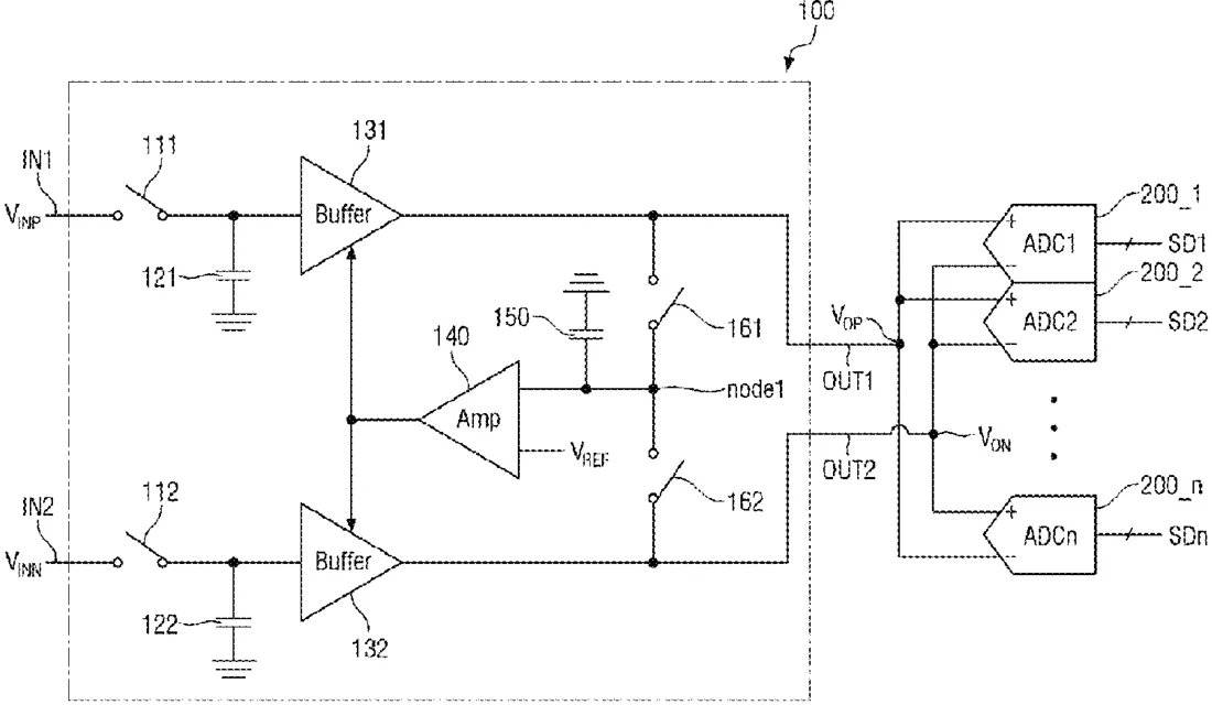
Samsung has patented a specific electronic circuit design used to capture and hold voltage levels before they are converted into digital data. The system uses buffers to manage the input signals and an amplifier that creates a feedback loop to keep the voltage levels stable and accurate.
In the filing’s own words
A sample-and-hold circuit includes first and second differential input terminals receiving distinct first and second differential input voltages. The sample-and-hold circuit also includes first and second unity gain buffers receiving, respectively, the first and second differential input voltages from the first and second differential input terminals. The sample-and-hold circuit includes an amplifier comparing received voltages and amplifying results of the comparison. The amplifier generates a feedback voltage which regulates outputs of the first and second unity gain buffers. The feedback voltage is based on a reference voltage and a common mode voltage that is provided from the first and second unity gain buffers.
What exactly they claim (claim 1)
1. A sample-and-hold circuit comprising: a first differential input terminal configured to receive a first differential input voltage among differential input voltages; a second differential input terminal configured to receive a second differential input voltage among the differential input voltages, which is different from the first differential input voltage; a first unity gain buffer configured to receive the first differential input voltage from the first differential input terminal and to output a first differential output voltage to a first differential output terminal; a second unity gain buffer configured to receive the second differential input voltage from the second differential input terminal and to output a second differential output voltage to a second differential output terminal; and an amplifier configured to compare received voltages and amplifying results of the comparison, wherein the amplifier is configured to compare a reference voltage and a common mode voltage generated by connecting output terminals of the first unity gain buffer and the second unity gain buffer, and to generate a feedback voltage based on a result of the comparison.
Facts
- Company
- Samsung (SAMSUNG ELECTRONICS CO., LTD.)
- Official title
- Sample-and-hold circuit and analog-to-digital converter circuit including the same
- Patent number
- US12756404B2
- Application number
- 18762277
- Filed
- Jul 2, 2024
- Granted
- Oct 6, 2026
- Inventors
- 4
- Claims
- 18
Classified under
H03M 3/02 Electricity & electronicsMore from Samsung in Chips & hardware
- Samsung patents chip that combines camera and screen Oct 13, 2026
- Samsung patents faster chip testing using machine learning Sep 1, 2026
- Samsung patents radar method to pinpoint target direction more accurately Sep 1, 2026
- Samsung patents memory chip that searches data by content, not address Sep 1, 2026
- Samsung patents chip design that skips empty data to speed up AI Sep 1, 2026
Summaries are simplified from the filing’s own abstract and first claim. A patent filing is not a product announcement.
Patent data and drawings: U.S. Patent and Trademark Office (USPTO). Nebula is not affiliated with or endorsed by the USPTO.