Samsung patents storage chip feature to adjust signal strength during startup
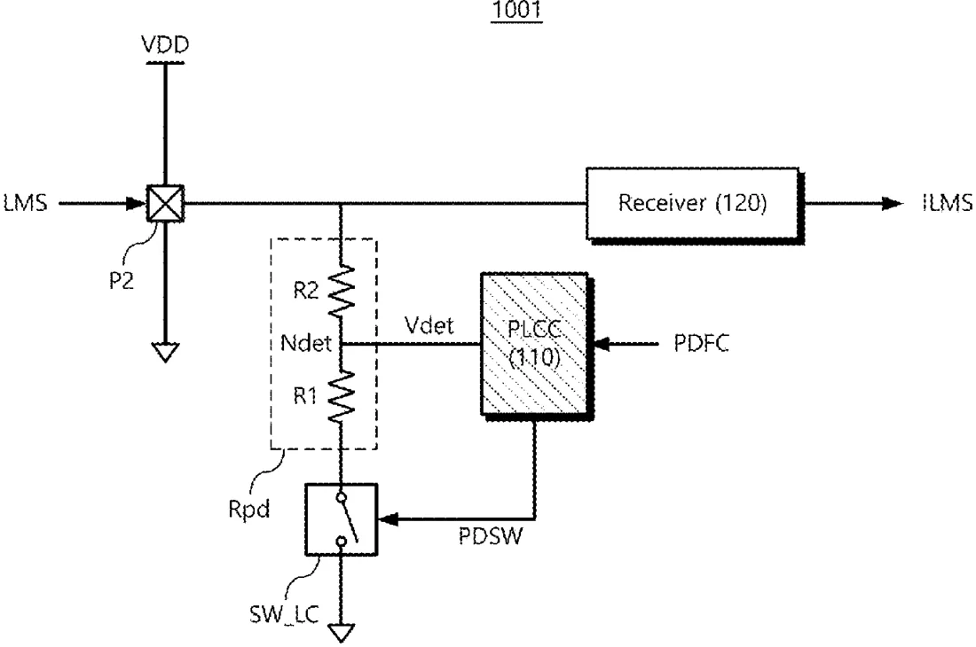
Samsung has been granted a patent for a storage device design that includes a specific circuit to manage how the chip connects to a computer or phone. The system uses a small resistor and a control circuit to adjust the voltage level of a signal pin, ensuring the device and the host agree on the correct communication mode when they first start up.
In the filing’s own words
A storage device including a non-volatile memory device; a memory controller controlling data input to the non-volatile memory device and data output from the non-volatile memory device; and a device interconnect layer transmitting signals received from a host to the memory controller. The device interconnect layer includes a first pad that inputs first data to be stored in the non-volatile memory device and that outputs second data stored in the non-volatile memory device; a second pad that receives a link startup mode signal from the host that indicates a link startup mode of the memory controller; a pull-down resistor between the second pad and a ground terminal; and a pad level control circuit that controls a voltage level of the second pad by controlling connection or disconnection of the pull-down resistor to the ground terminal based on the link startup mode signal.
What exactly they claim (claim 1)
1. A storage device comprising: a non-volatile memory device; a memory controller configured to control input of first data to the non-volatile memory device and output of second data from the non-volatile memory device; and a device interconnect layer configured to transmit signals received from a host to the memory controller, wherein the device interconnect layer comprises a first pad configured to input the first data to be stored in the non-volatile memory device and to output the second data from the non-volatile memory device, a second pad configured to receive a link startup mode signal from the host, the link startup mode signal being configured to cause the storage device to operate in a link startup mode, a pull-down resistor between the second pad and a ground terminal, and a pad level control circuit configured to control a voltage level of the second pad by controlling connection or disconnection of the pull-down resistor to the ground terminal based on the link startup mode signal.
Facts
- Company
- Samsung (Samsung Electronics Co., Ltd.)
- Official title
- Storage device including pad for determining link startup mode and method of controlling level of pad for determining link startup mode thereof
- Patent number
- US12756395B2
- Application number
- 18795795
- Filed
- Aug 6, 2024
- Granted
- Oct 6, 2026
- Inventors
- 4
- Claims
- 20
Classified under
H03K 19/1776 Electricity & electronicsH03K 19/01742 Electricity & electronicsMore from Samsung in Chips & hardware
- Samsung patents chip that combines camera and screen Oct 13, 2026
- Samsung patents faster chip testing using machine learning Sep 1, 2026
- Samsung patents radar method to pinpoint target direction more accurately Sep 1, 2026
- Samsung patents memory chip that searches data by content, not address Sep 1, 2026
- Samsung patents chip design that skips empty data to speed up AI Sep 1, 2026
Summaries are simplified from the filing’s own abstract and first claim. A patent filing is not a product announcement.
Patent data and drawings: U.S. Patent and Trademark Office (USPTO). Nebula is not affiliated with or endorsed by the USPTO.