Samsung patents plasma chamber that cools gas to treat chip packages
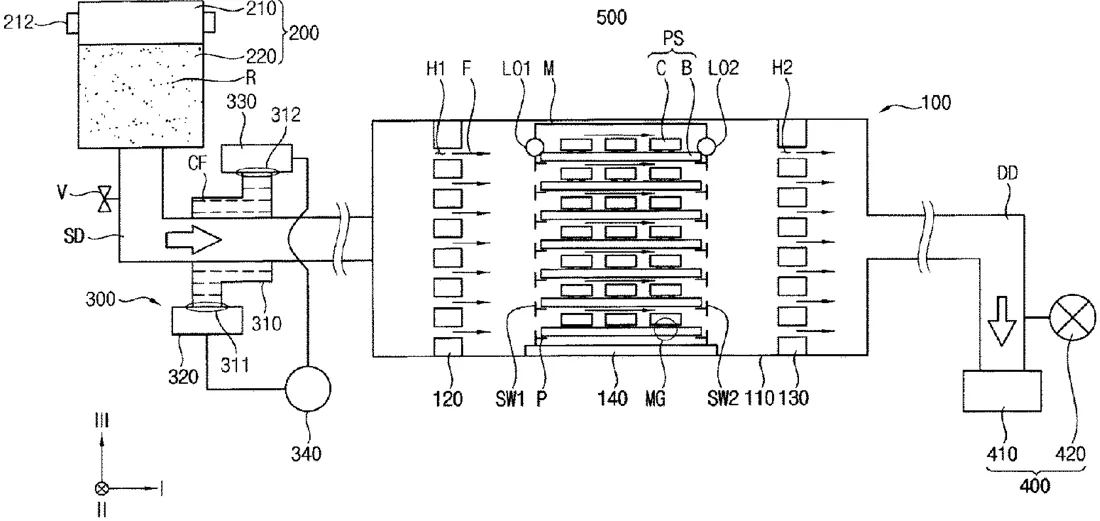
Samsung describes a machine that cleans the surfaces of semiconductor packages using a gas called plasma. The system generates the plasma outside the main chamber and cools it down before it enters, which helps prevent damage to the delicate chips inside. It also uses a grid of holes to control how the gas flows over stacked packages.
In the filing’s own words
A surface treatment apparatus and a surface treatment system having the same are disclosed. The surface treatment apparatus includes a process chamber in which the surface treatment process is conducted, a plasma generator for generating process radicals as a plasma state for the surface treatment process, the plasma generator being positioned outside of the process chamber and connected to the process chamber by a supply duct, a heat exchanger arranged on the supply duct and cooling down temperature of the process radicals passing through the supply duct and a flow controller controlling the process radicals to flow out of the process chamber. The flow controller is connected to a discharge duct through which the process radicals are discharged outside the process chamber. The plasma surface treatment process is conducted to the package structure having minute mounting gap without the damages to the IC chip and the board.
What exactly they claim (claim 1)
1. A method of manufacturing a semiconductor device, comprising: loading a plurality of package structures to a process chamber having first and second walls spaced apart in a first direction and a supply baffle and a discharge baffle adjacent to the first and the second walls, respectively, the supply and discharge baffles extending in a second direction perpendicular to the first direction, the supply baffle having a plurality of inlet holes and the discharge baffle having a plurality of outlet holes; after loading the plurality of package structures, selectively opening and closing the plurality of inlet holes and the plurality of outlet holes; supplying process radicals generated from an exterior plasma generator into the process chamber through the inlet holes to thereby conduct a plasma surface treatment process to surfaces of the package structures with the process radicals; and discharging the process radicals from the process chamber through the outlet holes, wherein the package structures are stacked in a third direction perpendicular to the first and second directions while the plasma surface treatment process is performed, wherein the plurality of inlet holes include a plurality of inlet hole rows, wherein the plurality of outlet holes include a plurality of outlet hole rows, and wherein selectively opening and closing the plurality of inlet holes and the plurality of outlet holes include simultaneously opening and closing the inlet hole rows and the outlet hole rows positioned at a same height.
Facts
- Company
- Samsung (Samsung Electronics Co., Ltd.)
- Official title
- Apparatus for conducting plasma surface treatment, board treatment system having the same, and method of manufacturing semiconductor devices using the same
- Patent number
- US12755942B2
- Application number
- 18217043
- Filed
- Jun 30, 2023
- Granted
- Oct 6, 2026
- Inventors
- 13
- Claims
- 20
Classified under
H01J 37/32449 Electricity & electronicsC23C 16/45504 Chemistry & metalsC23C 16/45589 Chemistry & metalsH01J 37/32633 Electricity & electronicsC23C 16/45502 Chemistry & metalsC23C 16/45591 Chemistry & metalsMore from Samsung in Chips & hardware
- Samsung patents chip that combines camera and screen Oct 13, 2026
- Samsung patents faster chip testing using machine learning Sep 1, 2026
- Samsung patents radar method to pinpoint target direction more accurately Sep 1, 2026
- Samsung patents memory chip that searches data by content, not address Sep 1, 2026
- Samsung patents chip design that skips empty data to speed up AI Sep 1, 2026
Summaries are simplified from the filing’s own abstract and first claim. A patent filing is not a product announcement.
Patent data and drawings: U.S. Patent and Trademark Office (USPTO). Nebula is not affiliated with or endorsed by the USPTO.