Samsung patents memory chip design with extra wiring to block interference
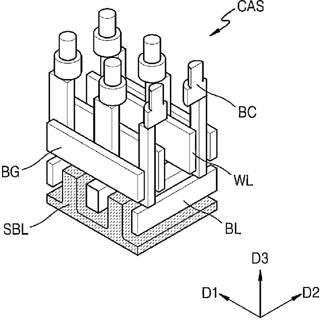
Samsung has been granted a patent for a memory device that uses a special 'shielding' wire placed underneath the main data lines. A control circuit switches this shield between different voltage levels to help the chip read data more accurately.
In the filing’s own words
A memory device includes a memory cell array, a sense amplifier, a voltage generation circuit and a control circuit. The memory cell array includes a plurality of bit lines to which a plurality of memory cells are connected, and a shielding bit line arranged between the plurality of bit lines and on lower portions of the plurality of bit lines. The sense amplifier is configured to sense and amplify data stored in a memory cell selected from among the plurality of memory cells. The voltage generation circuit is configured to generate a bit line precharge voltage and an internal power voltage based on a power voltage of the memory device. The control circuit is configured to selectively provide the shielding bit line with the bit line precharge voltage or the internal power voltage.
What exactly they claim (claim 1)
1. A memory device comprising: a memory cell array including: a plurality of bit lines extending in a second direction to which a plurality of memory cells are connected, and a shielding bit line including a plurality of bodies alternately arranged between the plurality of bit lines in a first direction crossing the second direction and below the plurality of bit lines in a third direction perpendicular to the first and second directions; a sense amplifier connected between a first sensing driving signal line and a second sensing driving signal line, and configured to sense and amplify data stored in a memory cell selected from among the plurality of memory cells; a voltage generation circuit configured to generate a bit line precharge voltage and an internal power voltage based on a power voltage of the memory device; and a control circuit configured to selectively provide the shielding bit line with the bit line precharge voltage, the internal power voltage, or a ground voltage, wherein a level of the internal power voltage is greater than a level of the bit line precharge voltage.
Facts
- Company
- Samsung (Samsung Electronics Co., Ltd.)
- Official title
- Memory device for controlling shielding bit lines
- Patent number
- US12755776B2
- Application number
- 18784796
- Filed
- Jul 25, 2024
- Granted
- Oct 6, 2026
- Inventors
- 8
- Claims
- 20
Classified under
G11C 11/4091 Physics & computingG11C 11/4094 Physics & computingMore from Samsung in Chips & hardware
- Samsung patents chip that combines camera and screen Oct 13, 2026
- Samsung patents faster chip testing using machine learning Sep 1, 2026
- Samsung patents radar method to pinpoint target direction more accurately Sep 1, 2026
- Samsung patents memory chip that searches data by content, not address Sep 1, 2026
- Samsung patents chip design that skips empty data to speed up AI Sep 1, 2026
Summaries are simplified from the filing’s own abstract and first claim. A patent filing is not a product announcement.
Patent data and drawings: U.S. Patent and Trademark Office (USPTO). Nebula is not affiliated with or endorsed by the USPTO.