Samsung patents memory that adjusts error-checking data size
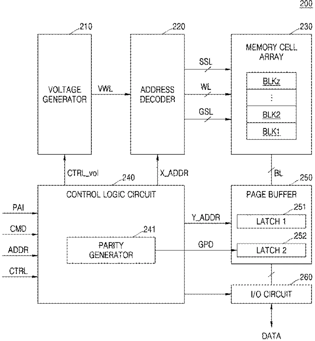
Samsung describes a memory device that changes the amount of error-checking data it stores based on instructions from an external controller. The system adjusts the size of these parity bits before moving them into a temporary buffer to match specific data formats.
In the filing’s own words
A memory device includes a memory cell array including a first memory region storing first data, a page buffer including a first latch configured to store data dumped from the memory cell array, and a control logic circuit configured to receive parity adjustment information from an external device and control an operation of the memory cell array. The first data includes first user data and first parity data including parity bits generated based on the first user data, and the control logic circuit dumps first parity data of which a size is adjusted based on the parity adjustment information to the first latch.
What exactly they claim (claim 1)
1. A memory device comprising: a memory cell array including a first memory region storing first data; a page buffer connected to the memory cell array and including a first latch configured to store data read from the memory cell array; and a control logic circuit configured to receive parity adjustment information from an external device and control an operation of the memory cell array, wherein the first data includes first user data and first parity data including parity bits generated based on the first user data, wherein the control logic circuit is configured to adjust a size of the first parity data, based on the parity adjustment information, and dump the adjusted first parity data to the first latch, and wherein the size of the first parity data dumped to the first latch varies depending on a format of the first parity data indicated by the parity adjustment information.
Facts
- Company
- Samsung (Samsung Electronics Co., Ltd.)
- Official title
- Memory device, memory controller, and storage device including the same
- Patent number
- US12754801B2
- Application number
- 18785327
- Filed
- Jul 26, 2024
- Granted
- Oct 6, 2026
- Inventors
- 3
- Claims
- 17
Classified under
G06F 11/1068 Physics & computingG06F 11/0778 Physics & computingG11C 7/106 Physics & computingMore from Samsung in Chips & hardware
- Samsung patents chip that combines camera and screen Oct 13, 2026
- Samsung patents faster chip testing using machine learning Sep 1, 2026
- Samsung patents radar method to pinpoint target direction more accurately Sep 1, 2026
- Samsung patents memory chip that searches data by content, not address Sep 1, 2026
- Samsung patents chip design that skips empty data to speed up AI Sep 1, 2026
Summaries are simplified from the filing’s own abstract and first claim. A patent filing is not a product announcement.
Patent data and drawings: U.S. Patent and Trademark Office (USPTO). Nebula is not affiliated with or endorsed by the USPTO.