Samsung patents circuit that stretches clock signals for chips
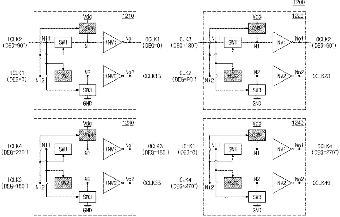
Samsung has been granted a patent for a circuit that changes the shape of clock signals used to synchronize computer chips. The design uses specific switches to create a signal with a longer active period than the original input.
In the filing’s own words
Disclosed is a clock converting circuit, which includes a first switch that is connected between a first input node for receiving a second input clock and a first node and operates in response to a first logic state of a first input clock, the second input clock delayed with respect to the first input clock as much as 90 degrees, a second switch that is connected between a second input node for receiving the first input clock and a second node and operates in response to a second logic state of the second input clock, and a third switch that is connected between the second node and a ground node and operates in response to a first logic state of the second input clock opposite to the second logic state of the second input clock.
What exactly they claim (claim 1)
1. A clock converting circuit comprising: a first switch connected between a first input node and a first node, and configured to receive a first input clock signal at the first input node and operate in response to a first logic state of a second input clock signal; and a second switch connected between a power node and the first node, and configured to operate in response to a second logic state of the second input clock signal, wherein the second switch includes a first PMOS transistor connected between the power node and the first node, wherein the first PMOS transistor is configured to provide a power voltage from the power node to the first node in response to the second logic state of the second input clock signal, wherein a voltage level of the power voltage of the power node is higher than a voltage level of a ground node, wherein the first PMOS transistor is configured to generate a voltage waveform at the first node with the first switch in response to the second input clock signal, and wherein a duty of the voltage waveform at the first node is longer than a duty of the first input clock signal.
Facts
- Company
- Samsung (Samsung Electronics Co., Ltd.)
- Official title
- Clock converting circuit with symmetric structure
- Patent number
- US12754585B2
- Application number
- 18196242
- Filed
- May 11, 2023
- Granted
- Oct 6, 2026
- Inventors
- 5
- Claims
- 19
Classified under
G06F 1/06 Physics & computingG06F 13/4022 Physics & computingG11C 11/403 Physics & computingG11C 11/40607 Physics & computingMore from Samsung in Chips & hardware
- Samsung patents chip that combines camera and screen Oct 13, 2026
- Samsung patents faster chip testing using machine learning Sep 1, 2026
- Samsung patents radar method to pinpoint target direction more accurately Sep 1, 2026
- Samsung patents memory chip that searches data by content, not address Sep 1, 2026
- Samsung patents chip design that skips empty data to speed up AI Sep 1, 2026
Summaries are simplified from the filing’s own abstract and first claim. A patent filing is not a product announcement.
Patent data and drawings: U.S. Patent and Trademark Office (USPTO). Nebula is not affiliated with or endorsed by the USPTO.