Samsung patents storage drive with separate side channel for management
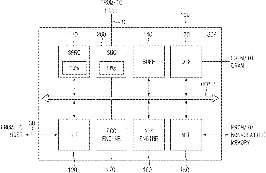
Samsung has been granted a patent for a storage system that connects a computer to a hard drive or SSD using two separate communication paths. The main path handles regular data transfers, while a secondary, lower-speed path allows the computer to send management commands directly to a small controller chip without interfering with the main data flow.
In the filing’s own words
A storage system includes a host device and a storage device that are connected to each other through a main link and a sub link. The storage device includes a nonvolatile memory device configured to store data and a storage controller package configured to control the nonvolatile memory device under control of the host device. The storage controller package includes an on-chip bus, a host interface connected to the on-chip bus and the main link, a memory interface connected to the on-chip bus and the nonvolatile memory device, a storage processor connected to the on-chip bus, and configured to perform an in-band communication with the host device through the on-chip bus, the host interface and the main link, and a microcontroller connected to the on-chip bus and the sub link, and configured to perform an out-of-band communication with the host device through the sub link.
What exactly they claim (claim 1)
1. A storage system comprising: a host device; and a storage device connected to the host device through both a main link and a sub link, wherein the storage device includes: a nonvolatile memory device configured to store data; and a storage controller package configured to control the nonvolatile memory device based on information from the host device, and wherein the storage controller package includes: an on-chip bus; a host interface connected to the on-chip bus and the main link; a memory interface connected to the on-chip bus and the nonvolatile memory device; a storage processor connected to the on-chip bus, and configured to access the nonvolatile memory device through the on-chip bus and to perform an in-band communication with the host device through the on-chip bus, the host interface and the main link; and a microcontroller connected to the on-chip bus and the sub link, and configured to access the nonvolatile memory device through the on-chip bus and to perform an out-of-band communication with the host device through the sub link.
Facts
- Company
- Samsung (SAMSUNG ELECTRONICS CO., LTD.)
- Official title
- Storage device and storage system including the same
- Patent number
- US12748694B2
- Application number
- 18973875
- Filed
- Dec 9, 2024
- Granted
- Sep 29, 2026
- Inventors
- 4
- Claims
- 20
Classified under
G06F 12/0246 Physics & computingMore from Samsung in Chips & hardware
- Samsung patents chip that combines camera and screen Oct 13, 2026
- Samsung patents faster chip testing using machine learning Sep 1, 2026
- Samsung patents radar method to pinpoint target direction more accurately Sep 1, 2026
- Samsung patents memory chip that searches data by content, not address Sep 1, 2026
- Samsung patents chip design that skips empty data to speed up AI Sep 1, 2026
Summaries are simplified from the filing’s own abstract and first claim. A patent filing is not a product announcement.
Patent data and drawings: U.S. Patent and Trademark Office (USPTO). Nebula is not affiliated with or endorsed by the USPTO.