Samsung patents storage check that maps data lines automatically
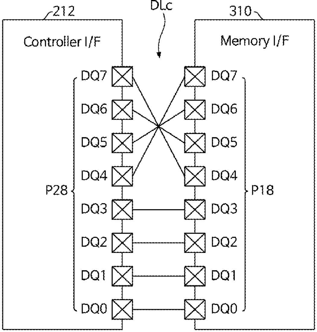
This patent describes a method where a storage controller sends a specific data pattern to a memory chip to verify the physical connections between them. The controller compares the expected pattern with what it actually receives to map out how the data pins are connected.
In the filing’s own words
A storage device comprising a storage controller including a plurality of first data pins and configured to send a command through a command/address (CA) line, the command including a first data pattern; and a memory device including a plurality of second data pins connected to the plurality of first data pins through a plurality of data lines, and configured to, in response to receiving the command from the storage controller, generate a second data pattern corresponding to the first data pattern based on the command, and send the second data pattern to the storage controller through the plurality of data lines, and the storage controller configured to receive a third data pattern in response to the memory device sending the second data pattern, and determine a connection structure between the plurality of first data pins and the plurality of second data pins based on the second and third data patterns.
What exactly they claim (claim 1)
1. A method of operating a storage device including a storage controller and a memory device, the method comprising: sending, by the storage controller, a command including a first data pattern, through a command/address line; generating, by the memory device, in response to receiving the command from the storage controller, a second data pattern corresponding to the first data pattern based on the command; sending, by the memory device, the second data pattern to the storage controller through a plurality of data lines; receiving, by the storage controller, in response to the memory device sending the second data pattern, a third data pattern; determining, by the storage controller, the second data pattern based on the command, independently from the memory device generating the second data pattern; and determining, by the storage controller, based on the second data pattern and the third data pattern, a connection structure between a plurality of first data pins of the storage controller and a plurality of second data pins of the memory device, the plurality of first data pins and the plurality of second data pins being connected to each other through the plurality of data lines.
Facts
- Company
- Samsung (Samsung Electronics Co., Ltd.)
- Official title
- Storage controller, storage device including the same, and operating method
- Patent number
- US12748688B2
- Application number
- 18957010
- Filed
- Nov 22, 2024
- Granted
- Sep 29, 2026
- Inventors
- 3
- Claims
- 20
Classified under
G06F 12/0223 Physics & computingG06F 13/1668 Physics & computingG11C 7/1006 Physics & computingMore from Samsung in Chips & hardware
- Samsung patents chip that combines camera and screen Oct 13, 2026
- Samsung patents faster chip testing using machine learning Sep 1, 2026
- Samsung patents radar method to pinpoint target direction more accurately Sep 1, 2026
- Samsung patents memory chip that searches data by content, not address Sep 1, 2026
- Samsung patents chip design that skips empty data to speed up AI Sep 1, 2026
Summaries are simplified from the filing’s own abstract and first claim. A patent filing is not a product announcement.
Patent data and drawings: U.S. Patent and Trademark Office (USPTO). Nebula is not affiliated with or endorsed by the USPTO.