Samsung patents memory chip that tracks data access to prevent wear
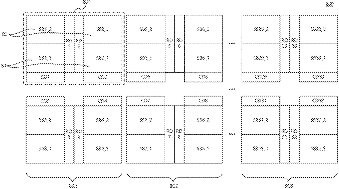
Samsung has been granted a patent for a memory design that splits storage into two sections: one for regular data and one for extra information about that data. The two sections are linked so the chip can count how often specific data lines are used, helping manage the physical wear on the memory cells.
In the filing’s own words
A memory device includes at least one bank including at least a first sub-bank and a second sub-bank disposed in a wordline direction. The first sub-bank may include a normal data region connected to a plurality of first wordlines and storing normal data, the second sub-bank may include a metadata region connected to a plurality of second wordlines and storing metadata corresponding to the normal data, the plurality of first wordlines may match the plurality of second wordlines to form a plurality of wordline pairs, and the first sub-bank and the second sub-bank may share a row hammer region storing a number of access times to the plurality of wordline pairs.
What exactly they claim (claim 1)
1. A memory device comprising at least one bank, the at least one bank comprising: a first sub-bank comprising: a plurality of first wordlines extending in a first direction; and a normal data region connected to the plurality of first wordlines, the normal data region configured to store normal data, a second sub-bank comprising: a plurality of second wordlines extending in the first direction; and a metadata region connected to the plurality of second wordlines, the metadata region configured to store metadata of the normal data, wherein the plurality of first wordlines and the plurality of second wordlines are matched to form a plurality of wordline pairs, and wherein the at least one bank further comprises a row hammer region shared by the first sub-bank and the second sub-bank, the row hammer region configured to store a number of times the plurality of wordline pairs are accessed.
Facts
- Company
- Samsung (SAMSUNG ELECTRONICS CO., LTD.)
- Official title
- Memory device and memory system
- Patent number
- US12748532B2
- Application number
- 18805709
- Filed
- Aug 15, 2024
- Granted
- Sep 29, 2026
- Inventors
- 4
- Claims
- 20
Classified under
G06F 3/0619 Physics & computingG06F 3/0659 Physics & computingG06F 3/0673 Physics & computingMore from Samsung in Chips & hardware
- Samsung patents chip that combines camera and screen Oct 13, 2026
- Samsung patents faster chip testing using machine learning Sep 1, 2026
- Samsung patents radar method to pinpoint target direction more accurately Sep 1, 2026
- Samsung patents memory chip that searches data by content, not address Sep 1, 2026
- Samsung patents chip design that skips empty data to speed up AI Sep 1, 2026
Summaries are simplified from the filing’s own abstract and first claim. A patent filing is not a product announcement.
Patent data and drawings: U.S. Patent and Trademark Office (USPTO). Nebula is not affiliated with or endorsed by the USPTO.