Sony patents camera sensor design with shared charge storage
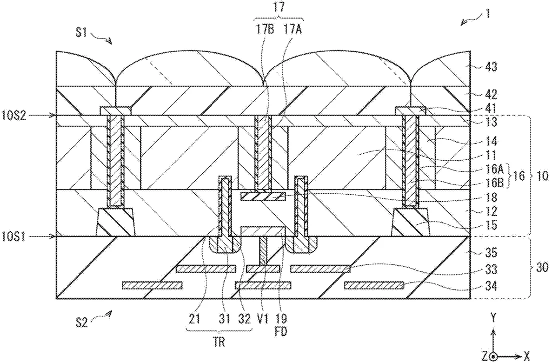
Sony describes a photodetector design where adjacent pixels share a storage area for electrical charges generated by light. The filing details a specific layout using grooves and an oxide film to manage how these charges are held and read out.
In the filing’s own words
A first imaging device according to an embodiment of the disclosure includes: a semiconductor substrate having opposing first and second surfaces, and including pixels arranged in matrix; photoelectric conversion sections formed to be embedded in the semiconductor substrate for the respective pixels and generating electric charge corresponding to a received light amount by photoelectric conversion; floating diffusion layers provided on the first surface between the adjacent pixels, and temporarily holding the electric charge generated in the photoelectric conversion sections provided for the respective adjacent pixels; a first groove part provided to surround the pixels sharing the floating diffusion layer and penetrating from the first surface to the second surface; a second groove part provided above at least the floating diffusion layers, stretching from the second surface toward the first surface, and having a bottom in the semiconductor substrate; and an oxide film provided in contact with the bottom.
What exactly they claim (claim 1)
1. A photodetector comprising: a semiconductor substrate having a first surface and a second surfaces opposed to each other, the semiconductor substrate including a plurality of pixels arranged in matrix; a plurality of photoelectric conversion sections formed to be embedded in the semiconductor substrate for the respective pixels and generating electric charge corresponding to a received light amount by photoelectric conversion; a plurality of floating diffusion layers provided on the first surface of the semiconductor substrate between the plurality of pixels adjacent to each other, the plurality of floating diffusion layers temporarily holding the electric charge generated in the plurality of photoelectric conversion sections provided for the respective pixels adjacent to each other; a first groove part provided to surround the plurality of pixels sharing corresponding one of the floating diffusion layers and penetrating from the first surface of the semiconductor substrate to the second surface; a second groove part provided above at least the plurality of floating diffusion layers and stretching from the second surface of the semiconductor substrate toward the first surface, the second groove part having a bottom in the semiconductor substrate; and an oxide film provided in contact with the bottom of the second groove part.
Facts
- Company
- Sony (SONY SEMICONDUCTOR SOLUTIONS CORPORATION)
- Official title
- PHOTODETECTOR
- Publication number
- US20260333916A1
- Application number
- 18880864
- Filed
- Jun 30, 2023
- Published
- Oct 22, 2026
- Inventors
- 9
- Claims
- 20
Classified under
H10F 39/807 Electricity & electronicsH10F 39/18 Electricity & electronicsH10F 39/813 Electricity & electronicsMore from Sony in Chips & hardware
- Sony patents light sensor that adjusts how it counts incoming photons Sep 1, 2026
- Sony patents camera sensor with two pixel types for better motion detection Sep 1, 2026
- Sony patents game graphics that adjust quality based on hardware heat Sep 8, 2026
- Sony patents camera sensor design that stacks chips to shrink pixels Sep 8, 2026
- Sony patents chip design that measures internal temperature from outside Sep 8, 2026
Summaries are simplified from the filing’s own abstract and first claim. A patent filing is not a product announcement.
Patent data and drawings: U.S. Patent and Trademark Office (USPTO). Nebula is not affiliated with or endorsed by the USPTO.