Sony patents camera sensor design using curved transistor channels
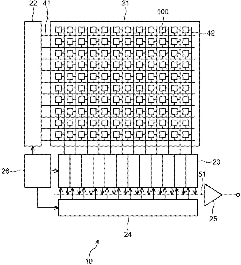
Sony has filed a patent for a camera sensor that uses transistors with curved, non-linear channels. The design uses a mask aligned with the gate electrode to inject impurities into these specific shapes to improve pixel performance.
In the filing’s own words
The present disclosure relates to a solid-state imaging device designed to improve the characteristics of pixels. There is provided a solid-state imaging device including a pixel array section having pixels arranged two-dimensionally therein, each of the pixels including a photoelectric conversion element and a pixel transistor. The pixel transistor includes a transistor having a structure in which impurities are injected into a nonlinear-shaped channel in planar view with use of a self-aligned mask corresponding to a gate electrode. The present disclosure can be applied to CMOS solid-state imaging devices, for example.
What exactly they claim (claim 1)
1. A solid-state imaging device comprising: a pixel array section having a plurality of pixels arranged two-dimensionally therein, each of the pixels including a photoelectric conversion element and a pixel transistor, wherein the pixel transistor includes a transistor having a structure in which impurities are injected into a nonlinear-shaped channel in planar view with use of a self-aligned mask corresponding to a gate electrode.
Facts
- Company
- Sony (SONY SEMICONDUCTOR SOLUTIONS CORPORATION)
- Official title
- SOLID-STATE IMAGING DEVICE
- Publication number
- US20260333907A1
- Application number
- 19117425
- Filed
- Sep 21, 2023
- Published
- Oct 22, 2026
- Inventors
- 4
- Claims
- 22
Classified under
H10F 39/80377 Electricity & electronicsMore from Sony in Chips & hardware
- Sony patents light sensor that adjusts how it counts incoming photons Sep 1, 2026
- Sony patents camera sensor with two pixel types for better motion detection Sep 1, 2026
- Sony patents game graphics that adjust quality based on hardware heat Sep 8, 2026
- Sony patents camera sensor design that stacks chips to shrink pixels Sep 8, 2026
- Sony patents chip design that measures internal temperature from outside Sep 8, 2026
Summaries are simplified from the filing’s own abstract and first claim. A patent filing is not a product announcement.
Patent data and drawings: U.S. Patent and Trademark Office (USPTO). Nebula is not affiliated with or endorsed by the USPTO.