Nvidia patents stacked chip design for faster AI math
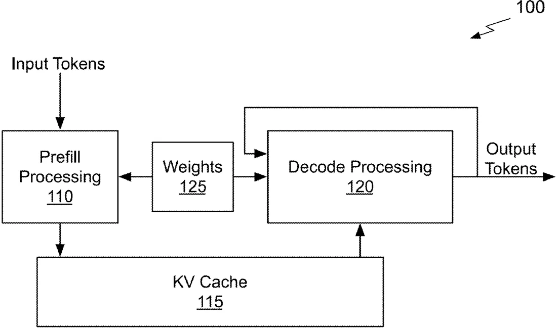
Nvidia describes a chip design where the processing unit is physically stacked on top of memory to reduce the time data takes to move between them. It uses specialized sections to handle different parts of AI calculations in parallel, allowing for quicker results without moving data back and forth as often.
In the filing’s own words
A low-latency processing system reduces data movement, improves memory bandwidth utilization, and enables, e.g., scalable, low-latency neural network inference. Compute tiles are configured to efficiently execute activation functions in parallel. IMLP tiles efficiently perform data format conversions and reduction operations as part of intermediate layer processing. A configurable network transmits data directly from source to destination register(s) within compute and IMLP tiles. Connections are, e.g., pre-configured for one or more cycles of neural network inference. The low-latency inference device may be stacked with one or more memory die for storing tensor inputs, KV cache data, activations, and other neural network-related information required for inference.
What exactly they claim (claim 1)
1. A method of performing a tensor operation using a low-latency inference low-latency inference (LLI) device stacked with one or more memory dies, comprising: transmitting, by one or more compute tiles fabricated in the LLI device, a read request generated by one or more memory read interfaces within the one or more compute tiles via first electrical contacts to the one or more memory dies to retrieve one or more tensor inputs stored in the one or more memory dies; processing, by the one or more compute tiles, the one or more tensor inputs retrieved from the one or more memory dies to generate one or more partial results; transmitting, via a configurable network, the one or more partial results from the one or more compute tiles to at least one inter-matrix layer processing (IMLP) tile fabricated in the LLI device; processing, by the at least one IMLP tile, the one or more partial results to generate one or more reduced results; and transmitting, by the at least one IMLP tile, a write request generated by a memory write interface within the at least one IMLP tile via second electrical contacts to the one or more memory dies to store the reduced results in the one or more memory dies.
Facts
- Company
- Nvidia (NVIDIA Corporation)
- Official title
- STACKED MEMORY LOW-LATENCY COMPUTE ARCHITECTURES AND USE FOR NEURAL NETWORK INFERENCE
- Publication number
- US20260330261A1
- Application number
- 19453587
- Filed
- Jan 20, 2026
- Published
- Oct 22, 2026
- Inventors
- 4
- Claims
- 20
Classified under
G06N 5/04 Physics & computingMore from Nvidia in Chips & hardware
- Nvidia patents method to skip zero data in neural network math Oct 13, 2026
- Nvidia patents hardware to speed up motion blur in ray tracing Oct 13, 2026
- Nvidia patents method to sync data across split processor chips Sep 17, 2026
- Nvidia patents chip math trick to speed up AI calculations Oct 8, 2026
- Nvidia patents data center cooling that uses cryogenic fluids Oct 15, 2026
Summaries are simplified from the filing’s own abstract and first claim. A patent filing is not a product announcement.
Patent data and drawings: U.S. Patent and Trademark Office (USPTO). Nebula is not affiliated with or endorsed by the USPTO.