Sony patents camera sensor design with stacked wiring for better images
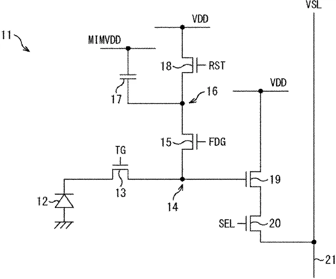
Sony describes a camera sensor design where a specific capacitor is built between wiring layers to store electrical charge from light. The filing explains that a wire covers the entire second electrode of this capacitor when viewed from the top logic layer. This structure is intended to improve image quality in stacked CMOS image sensors.
In the filing’s own words
The present disclosure relates to a solid-state imaging element and an electronic device that are capable of achieving more improved image quality. The solid-state imaging element includes, for each pixel, a photoelectric conversion unit that photoelectrically converts light into an electric charge; a first FD section that accumulates the electric charge transferred from the photoelectric conversion unit via a transfer transistor to convert the electric charge into a pixel signal; a second FD section that is connected to the first FD section via a connection transistor; and an inter-wire capacitor that is connected to the second FD section to accumulate the electric charge. In addition, the inter-wire capacitor is configured to include a first electrode that is connected to the second FD section and a second electrode that faces the first electrode across a dielectric, and when viewed in a plan view from a logic substrate that is stacked on a sensor substrate on which the photoelectric conversion unit is provided, a wire connected to the second electrode is provided to cover at least the entire second electrode. The present technology can be applied to, for example, a CMOS image sensor with a stacked structure.
What exactly they claim (claim 1)
1. A solid-state imaging element comprising: for each pixel, a photoelectric conversion unit that photoelectrically converts light into an electric charge; a first FD (Floating Diffusion) section that accumulates the electric charge transferred from the photoelectric conversion unit via a transfer transistor to convert the electric charge into a pixel signal; a second FD section that is connected to the first FD section via a connection transistor; and an inter-wire capacitor that is connected to the second FD section to accumulate the electric charge, wherein the inter-wire capacitor is configured to include a first electrode that is connected to the second FD section and a second electrode that faces the first electrode across a dielectric, and when viewed in a plan view from a logic substrate that is stacked on a sensor substrate on which the photoelectric conversion unit is provided, a wire connected to the second electrode is provided to cover at least the entire second electrode.
Facts
- Company
- Sony (SONY SEMICONDUCTOR SOLUTIONS CORPORATION)
- Official title
- SOLID-STATE IMAGING ELEMENT AND ELECTRONIC DEVICE
- Publication number
- US20260324108A1
- Application number
- 19104260
- Filed
- Aug 8, 2023
- Published
- Oct 15, 2026
- Inventors
- 1
- Claims
- 12
Classified under
H10F 39/8037 Electricity & electronicsH04N 25/628 Electricity & electronicsH04N 25/771 Electricity & electronicsH04N 25/772 Electricity & electronicsH04N 25/79 Electricity & electronicsH10F 39/811 Electricity & electronicsMore from Sony in Chips & hardware
- Sony patents light sensor that adjusts how it counts incoming photons Sep 1, 2026
- Sony patents camera sensor with two pixel types for better motion detection Sep 1, 2026
- Sony patents game graphics that adjust quality based on hardware heat Sep 8, 2026
- Sony patents camera sensor design that stacks chips to shrink pixels Sep 8, 2026
- Sony patents chip design that measures internal temperature from outside Sep 8, 2026
Summaries are simplified from the filing’s own abstract and first claim. A patent filing is not a product announcement.
Patent data and drawings: U.S. Patent and Trademark Office (USPTO). Nebula is not affiliated with or endorsed by the USPTO.