Sony patents camera sensor design that uses side walls for storage
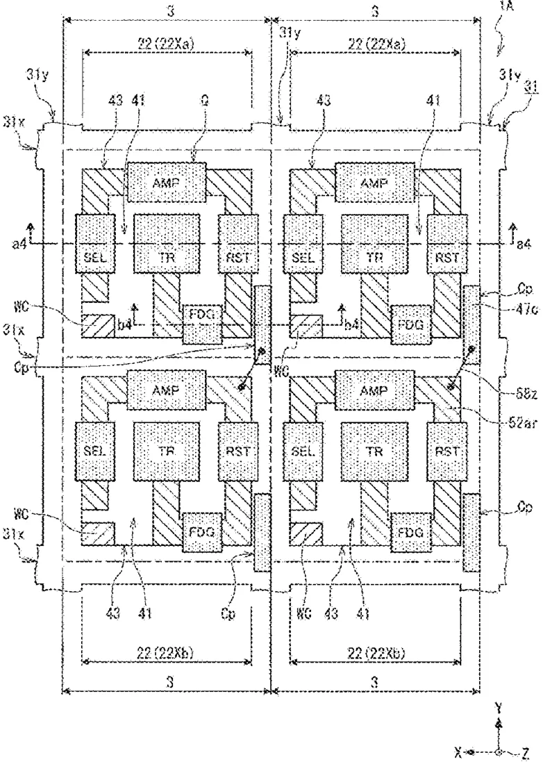
Sony has filed a patent for a photodetection device that arranges components differently within a camera sensor. Instead of placing all parts on the flat top surface, the design uses the vertical side walls of the sensor's active area to hold a capacitive element. This component helps store the electrical charge created when light hits the sensor.
In the filing’s own words
To increase a degree of freedom in arrangement of elements in a photoelectric conversion region. A photodetection device includes a semiconductor layer including a photoelectric conversion region that has a first surface portion and a second surface portion located opposite to each other in a thickness direction and is partitioned by an isolation region extending in the thickness direction. Then, the photoelectric conversion region includes: an upper surface portion located on the first surface portion side of the semiconductor layer; a side surface portion located on the isolation region side; a pixel transistor provided on the upper surface portion side; a floating diffusion region that is provided on the upper surface portion side and holds a signal charge photoelectrically converted by the photoelectric conversion unit; and a capacitive element connected to the floating diffusion region. Then, the capacitive element includes: a first electrode provided in the isolation region adjacent to the side surface portion of the photoelectric conversion region with a dielectric film interposed therebetween; and a second electrode provided adjacent to the first electrode inside the side surface portion of the photoelectric conversion region.
What exactly they claim (claim 1)
1. A photodetection device comprising a semiconductor layer including a photoelectric conversion region that has a first surface portion and a second surface portion located opposite to each other in a thickness direction and is partitioned by an isolation region extending in the thickness direction, wherein the photoelectric conversion region includes: an upper surface portion located on the first surface portion side of the semiconductor layer; a side surface portion located on the isolation region side; a pixel transistor provided on the upper surface portion side; a floating diffusion region that is provided on the upper surface portion side and holds a signal charge photoelectrically converted by the photoelectric conversion unit; and a capacitive element connected to the floating diffusion region, and the capacitive element includes: a first electrode provided in the isolation region adjacent to the side surface portion of the photoelectric conversion region with a dielectric film interposed therebetween; and a second electrode provided adjacent to the first electrode inside the side surface portion of the photoelectric conversion region.
Facts
- Company
- Sony (SONY SEMICONDUCTOR SOLUTIONS CORPORATION)
- Official title
- PHOTODETECTION DEVICE AND ELECTRONIC APPARATUS
- Publication number
- US20260324106A1
- Application number
- 19491498
- Filed
- May 13, 2024
- Published
- Oct 15, 2026
- Inventors
- 1
- Claims
- 9
Classified under
H10F 39/8023 Electricity & electronicsH10F 30/221 Electricity & electronicsH10F 39/182 Electricity & electronicsH10F 39/8027 Electricity & electronicsH10F 39/8033 Electricity & electronicsH10F 39/80373 Electricity & electronicsMore from Sony in Chips & hardware
- Sony patents light sensor that adjusts how it counts incoming photons Sep 1, 2026
- Sony patents camera sensor with two pixel types for better motion detection Sep 1, 2026
- Sony patents game graphics that adjust quality based on hardware heat Sep 8, 2026
- Sony patents camera sensor design that stacks chips to shrink pixels Sep 8, 2026
- Sony patents chip design that measures internal temperature from outside Sep 8, 2026
Summaries are simplified from the filing’s own abstract and first claim. A patent filing is not a product announcement.
Patent data and drawings: U.S. Patent and Trademark Office (USPTO). Nebula is not affiliated with or endorsed by the USPTO.