Sony patents camera sensor design to cut power use during image capture
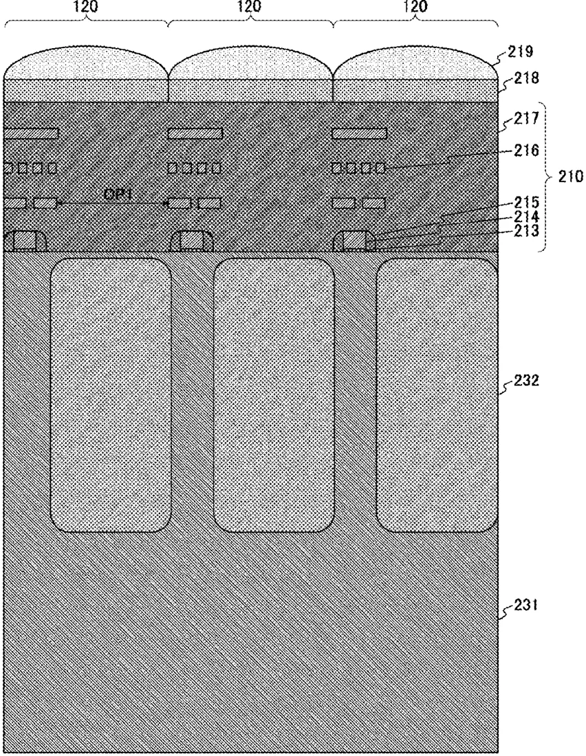
Sony has filed a patent for an imaging device that manages the electrical load on its sensor's signal lines. The design includes a specific voltage generator connected to the signal path to help read data from pixels without drawing too much power or taking too long to stabilize.
In the filing’s own words
Capacitive load reading is enabled while suppressing an increase in current consumption and settling time. An imaging device includes: a signal line that changes in potential on the basis of a charge accumulated according to a current passing when a signal is read from a pixel; a signal line transistor electrically connected to the signal line; and a voltage generation unit connected in series to the signal line transistor and being capable of generating a voltage higher than 0 V. The pixel may include a photodiode; a transfer transistor that transfers a charge accumulated in the photodiode to a floating diffusion; a reset transistor that resets the floating diffusion; an amplification transistor that outputs a signal corresponding to the potential of the floating diffusion; and a selection transistor connected between the amplification transistor and the signal line.
What exactly they claim (claim 1)
1. An imaging device comprising: a signal line that changes in potential on the basis of a charge accumulated according to a current passing when a signal is read from a pixel; a signal line transistor electrically connected to the signal line; and a voltage generation unit connected in series to the signal line transistor and being capable of generating a voltage higher than 0 V.
Facts
- Company
- Sony (SONY SEMICONDUCTOR SOLUTIONS CORPORATION)
- Official title
- IMAGING DEVICE
- Publication number
- US20260323189A1
- Application number
- 19104312
- Filed
- Jun 30, 2023
- Published
- Oct 15, 2026
- Inventors
- 3
- Claims
- 20
Classified under
H04N 25/78 Electricity & electronicsH04N 25/709 Electricity & electronicsH04N 25/772 Electricity & electronicsMore from Sony in Chips & hardware
- Sony patents light sensor that adjusts how it counts incoming photons Sep 1, 2026
- Sony patents camera sensor with two pixel types for better motion detection Sep 1, 2026
- Sony patents game graphics that adjust quality based on hardware heat Sep 8, 2026
- Sony patents camera sensor design that stacks chips to shrink pixels Sep 8, 2026
- Sony patents chip design that measures internal temperature from outside Sep 8, 2026
Summaries are simplified from the filing’s own abstract and first claim. A patent filing is not a product announcement.
Patent data and drawings: U.S. Patent and Trademark Office (USPTO). Nebula is not affiliated with or endorsed by the USPTO.