Sony patents stacked chip design for faster optical data receivers
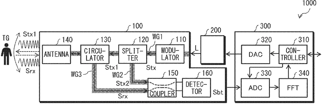
Sony describes a receiver that combines a silicon chip handling light with a separate chip processing electrical signals. The two chips are stacked directly on top of each other to shorten the distance data must travel. A specific pattern etched into the silicon helps direct light in and out of the device.
In the filing’s own words
An optical receiver according to an embodiment of the present disclosure includes a PIC substrate and a signal processing substrate. The PIC substrate includes a first waveguide and an antenna. The first waveguide is configured to transmit a transmission signal. The antenna is configured to output the transmission signal to an outside via an entrance-and-exit surface and to receive a return signal from the outside via the entrance-and-exit surface. The PIC substrate and the signal processing substrate are stacked on each other and are electrically coupled to each other via a joining surface between the PIC substrate and the signal processing substrate. The antenna includes a first diffraction grating provided in a region between the Si layer and the entrance-and-exit surface.
What exactly they claim (claim 1)
1. An optical receiver, comprising: a PIC (Photonic Integration Circuit) substrate that includes a first waveguide and an antenna and in which the first waveguide and a part of the antenna are provided in a common Si (Silicon) layer, and in addition, an entrance-and-exit surface is provided at a location opposed to the antenna, the first waveguide being configured to transmit a transmission signal, the antenna being configured to output the transmission signal to an outside via the entrance-and-exit surface and to receive a return signal from the outside via the entrance-and-exit surface; and a signal processing substrate configured to process a signal generated on a basis of the return signal, wherein the PIC substrate and the signal processing substrate are stacked on each other and are electrically coupled to each other via a joining surface between the PIC substrate and the signal processing substrate, and the antenna includes a first diffraction grating provided in a region between the Si layer and the entrance-and-exit surface.
Facts
- Company
- Sony (SONY SEMICONDUCTOR SOLUTIONS CORPORATION)
- Official title
- OPTICAL RECEIVER
- Publication number
- US20260322500A1
- Application number
- 19481056
- Filed
- May 15, 2024
- Published
- Oct 15, 2026
- Inventors
- 1
- Claims
- 5
Classified under
H04B 10/66 Electricity & electronicsG02B 6/124 Physics & computingG02B 2006/12107 Physics & computingMore from Sony in Chips & hardware
- Sony patents light sensor that adjusts how it counts incoming photons Sep 1, 2026
- Sony patents camera sensor with two pixel types for better motion detection Sep 1, 2026
- Sony patents game graphics that adjust quality based on hardware heat Sep 8, 2026
- Sony patents camera sensor design that stacks chips to shrink pixels Sep 8, 2026
- Sony patents chip design that measures internal temperature from outside Sep 8, 2026
Summaries are simplified from the filing’s own abstract and first claim. A patent filing is not a product announcement.
Patent data and drawings: U.S. Patent and Trademark Office (USPTO). Nebula is not affiliated with or endorsed by the USPTO.