Sony patents compact light source that adjusts its power output
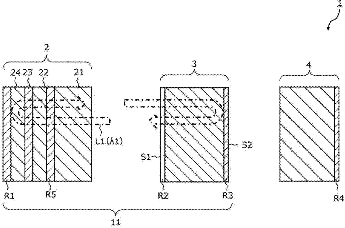
Sony describes a small light source device that combines a semiconductor layer with a laser medium to emit light at specific wavelengths. The design uses multiple reflection layers to control the light path, allowing the device to vary its peak power while remaining compact.
In the filing’s own words
[Problem] A light source device can be miniaturized and can vary peak power. [Means of Solution] The light source device includes: a laminated semiconductor layer that includes an active layer that emits light of a first wavelength that is a wavelength that changes according to a driving condition, and a first reflection layer that is used for the first wavelength: a second reflection layer that is disposed on a first surface facing a light emission surface of the laminated semiconductor layer, and is used for a second wavelength; a third reflection layer that is disposed on a second surface disposed closer to a rear side of an optical axis than the first surface, and is used for the first wavelength; a laser medium that is disposed between the second reflection layer and the third reflection layer; a fourth reflection layer that is disposed on the second surface or is disposed closer to the rear side of the optical axis than the second surface and is used for the second wavelength; and a first resonator that resonates the light of the first wavelength between the first reflection layer and the third reflection layer, and an optical axis of the laminated semiconductor layer and an optical axis of the laser medium are arranged uniaxially.
What exactly they claim (claim 1)
1. A light source device comprising: a laminated semiconductor layer that includes an active layer that emits light of a first wavelength that is a wavelength that changes according to a driving condition, and a first reflection layer that is used for the first wavelength; a second reflection layer that is disposed on a first surface facing a light emission surface of the laminated semiconductor layer, and is used for a second wavelength; a third reflection layer that is disposed on a second surface disposed closer to a rear side of an optical axis than the first surface, and is used for the first wavelength; a laser medium that is disposed between the second reflection layer and the third reflection layer; a fourth reflection layer that is disposed on the second surface or is disposed closer to the rear side of the optical axis than the second surface and is used for the second wavelength; and a first resonator that resonates the light of the first wavelength between the first reflection layer and the third reflection layer, wherein an optical axis of the laminated semiconductor layer and an optical axis of the laser medium are arranged uniaxially.
Facts
- Company
- Sony (SONY GROUP CORPORATION)
- Official title
- LIGHT SOURCE DEVICE, RANGING DEVICE, AND RANGING METHOD
- Publication number
- US20260322071A1
- Application number
- 19105491
- Filed
- Aug 18, 2023
- Published
- Oct 15, 2026
- Inventors
- 2
- Claims
- 20
Classified under
H01S 5/042 Electricity & electronicsH01S 3/0941 Electricity & electronicsH01S 3/113 Electricity & electronicsMore from Sony in Chips & hardware
- Sony patents light sensor that adjusts how it counts incoming photons Sep 1, 2026
- Sony patents camera sensor with two pixel types for better motion detection Sep 1, 2026
- Sony patents game graphics that adjust quality based on hardware heat Sep 8, 2026
- Sony patents camera sensor design that stacks chips to shrink pixels Sep 8, 2026
- Sony patents chip design that measures internal temperature from outside Sep 8, 2026
Summaries are simplified from the filing’s own abstract and first claim. A patent filing is not a product announcement.
Patent data and drawings: U.S. Patent and Trademark Office (USPTO). Nebula is not affiliated with or endorsed by the USPTO.