Sony patents camera sensor design with stacked layers and connecting plugs
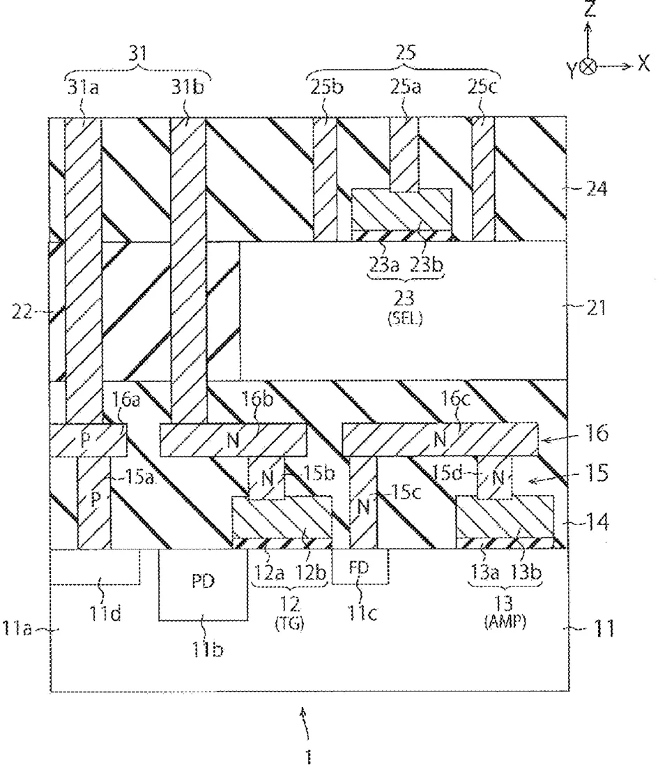
Sony has filed a patent for a solid-state imaging device, which is the type of sensor used in cameras. The design stacks a second substrate on top of a first one, using small plugs to connect electrical wires between the layers.
In the filing’s own words
To provide a solid-state imaging device capable of suitably disposing a plug in a substrate, and a manufacturing method of the solid-state imaging device. A solid-state imaging device of the present disclosure includes a first substrate, a first transistor provided on the first substrate, a first insulating film provided on the first substrate and the first transistor, a first wiring provided in the first insulating film and electrically connected to the first substrate or the first transistor, a second substrate provided on the first insulating film, and a first plug provided in the first insulating film and the second substrate and provided on the first wiring to be electrically connected to the first wiring.
What exactly they claim (claim 1)
1. A solid-state imaging device, comprising: a first substrate; a first transistor provided on the first substrate; a first insulating film provided on the first substrate and the first transistor; a first wiring provided in the first insulating film and electrically connected to the first substrate or the first transistor; a second substrate provided on the first insulating film; and a first plug provided in the first insulating film and the second substrate and provided on the first wiring to be electrically connected to the first wiring.
Facts
- Company
- Sony (SONY SEMICONDUCTOR SOLUTIONS CORPORATION)
- Official title
- SOLID-STATE IMAGING DEVICE AND MANUFACTURING METHOD OF THE SAME
- Publication number
- US20260304993A1
- Application number
- 18996300
- Filed
- Jun 1, 2023
- Published
- Oct 1, 2026
- Inventors
- 1
- Claims
- 20
Classified under
H10F 39/811 Electricity & electronicsH10F 39/014 Electricity & electronicsH10F 39/18 Electricity & electronicsH10F 39/199 Electricity & electronicsH10F 39/8037 Electricity & electronicsH10F 39/806 Electricity & electronicsMore from Sony in Chips & hardware
- Sony patents light sensor that adjusts how it counts incoming photons Sep 1, 2026
- Sony patents camera sensor with two pixel types for better motion detection Sep 1, 2026
- Sony patents game graphics that adjust quality based on hardware heat Sep 8, 2026
- Sony patents camera sensor design that stacks chips to shrink pixels Sep 8, 2026
- Sony patents chip design that measures internal temperature from outside Sep 8, 2026
Summaries are simplified from the filing’s own abstract and first claim. A patent filing is not a product announcement.
Patent data and drawings: U.S. Patent and Trademark Office (USPTO). Nebula is not affiliated with or endorsed by the USPTO.