Sony patents camera sensor circuit that adjusts power for better image quality
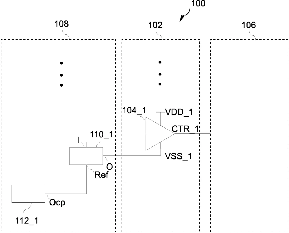
Sony has filed a patent for a specific circuit design used in digital camera sensors. The system uses a voltage regulator and a charge pump to manage the power supplied to the lines that read data from the sensor's pixels.
In the filing’s own words
A row driver assembly includes a row driver unit having a plurality of buffer circuits, each buffer circuit including a high buffer supply input and a low buffer supply input and configured to drive a control signal to a pixel circuit that converts incident radiation into an electric signal. A voltage converter unit is coupled to the low buffer supply inputs and includes a voltage regulator circuit and a charge pump circuit. The voltage regulator circuit has an input, an output, and a reference input, with the output coupled to a low buffer supply input of a first buffer circuit. The charge pump circuit has an output coupled to the reference input of the voltage regulator circuit.
What exactly they claim (claim 1)
1. A row driver assembly, comprising: a row driver unit comprising n buffer circuits, n being an integer larger than 1, wherein each of the n buffer circuits includes a high buffer supply input and a low buffer supply input, and is configured to drive a buffered control signal to a pixel circuit configured to convert incident radiation into an electric signal; a voltage converter unit electrically coupled to low buffer supply inputs of the n buffer circuits, the voltage converter unit including a voltage regulator circuit comprising an input, an output, and a reference input, wherein the output of the voltage regulator circuit is electrically coupled to a low buffer supply input of a first buffer circuit of the n buffer circuits; and a charge pump circuit, wherein an output of the charge pump circuit is electrically coupled to the reference input of the voltage regulator circuit.
Facts
- Company
- Sony (Sony Semiconductor Solutions Corporation)
- Official title
- ROW DRIVER ASSEMBLY AND SOLID-STATE IMAGING DEVICE
- Publication number
- US20260303992A1
- Application number
- 19164243
- Filed
- Mar 7, 2024
- Published
- Oct 1, 2026
- Inventors
- 2
- Claims
- 13
Classified under
H04N 25/709 Electricity & electronicsG05F 1/46 Physics & computingH02M 3/07 Electricity & electronicsH04N 25/779 Electricity & electronicsH04N 25/79 Electricity & electronicsMore from Sony in Chips & hardware
- Sony patents light sensor that adjusts how it counts incoming photons Sep 1, 2026
- Sony patents camera sensor with two pixel types for better motion detection Sep 1, 2026
- Sony patents game graphics that adjust quality based on hardware heat Sep 8, 2026
- Sony patents camera sensor design that stacks chips to shrink pixels Sep 8, 2026
- Sony patents chip design that measures internal temperature from outside Sep 8, 2026
Summaries are simplified from the filing’s own abstract and first claim. A patent filing is not a product announcement.
Patent data and drawings: U.S. Patent and Trademark Office (USPTO). Nebula is not affiliated with or endorsed by the USPTO.