Sony patents circuit board design that separates wireless antennas with a cut
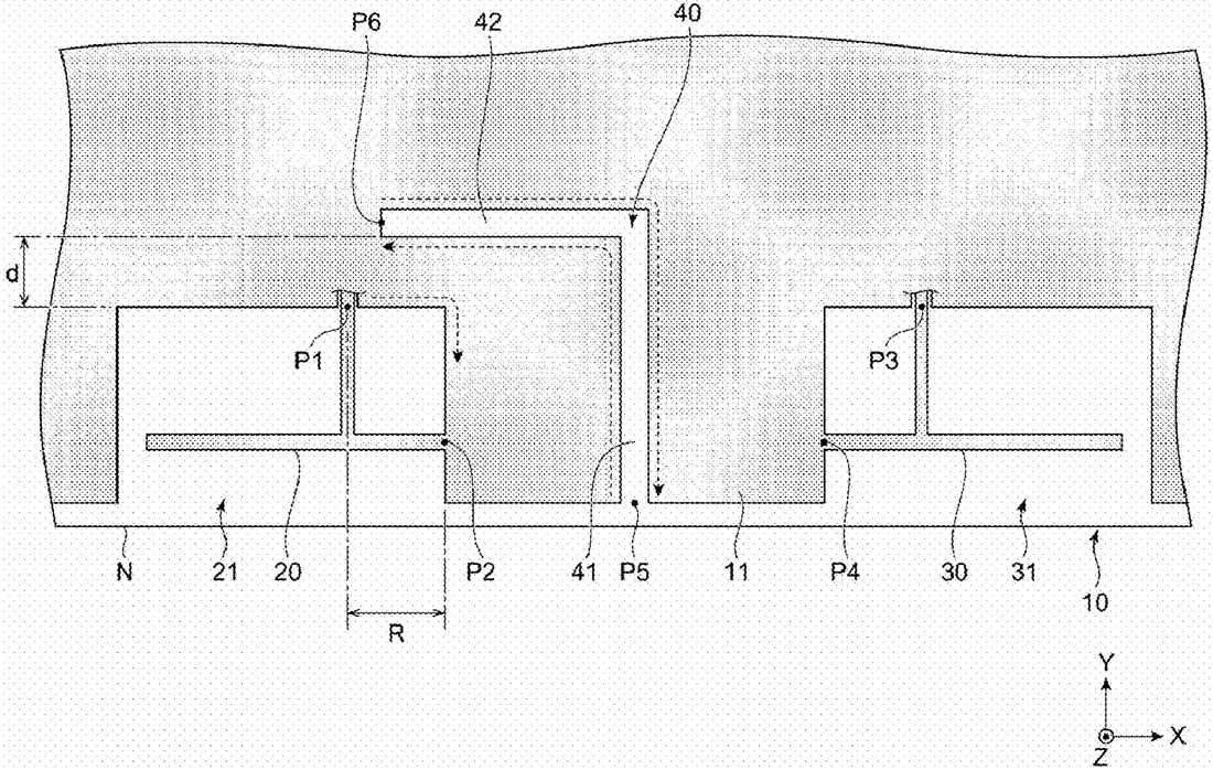
Sony describes an electronic device with two wireless antennas placed on a flat circuit board. The design uses a specific cut in the metal ground layer to separate the antennas and prevent them from interfering with each other.
In the filing’s own words
Provided is an electronic device including a substrate ( 10), a first antenna ( 20) and a second antenna ( 30) formed on the substrate ( 10) and each configured to perform wireless communication, a ground pattern ( 11) formed by a single conductor layer of the substrate ( 10), and a slit ( 40) formed by cutting out the conductor layer, with a base point that is a point on an outer periphery of the ground pattern ( 11), in which the first antenna ( 20) is disposed within a first antenna region ( 21) surrounded by an outer periphery of the substrate ( 10) and the conductor layer in plan view, the second antenna ( 30) is disposed within a second antenna region ( 31) surrounded by the outer periphery of the substrate ( 10) and the conductor layer in plan view, the base point of the slit ( 40) is located between the first antenna region ( 21) and the second antenna region ( 31) in plan view, and the slit ( 40) has a portion opposing an end portion on a side opposite to a side of the outer periphery of the substrate ( 10) of the first antenna region ( 21) in plan view.
What exactly they claim (claim 1)
1. An electronic device comprising: a substrate; a first antenna and a second antenna formed on the substrate and each configured to perform wireless communication; a ground pattern formed by a single conductor layer of the substrate; and a slit formed by cutting out the conductor layer, with a base point that is a point on an outer periphery of the ground pattern, wherein the first antenna is disposed within a first antenna region surrounded by an outer periphery of the substrate and the conductor layer in a plan view, the second antenna is disposed within a second antenna region surrounded by the outer periphery of the substrate and the conductor layer in the plan view, the base point of the slit is located between the first antenna region and the second antenna region in the plan view, and the slit has a portion opposing an end portion on a side opposite to a side of the outer periphery of the substrate of the first antenna region in the plan view.
Facts
- Company
- Sony (Sony Interactive Entertainment Inc.)
- Official title
- ELECTRONIC DEVICE
- Publication number
- US20260302609A1
- Application number
- 19475640
- Filed
- Apr 21, 2023
- Published
- Oct 1, 2026
- Inventors
- 3
- Claims
- 20
Classified under
H01Q 1/528 Electricity & electronicsH01Q 1/48 Electricity & electronicsH01Q 1/521 Electricity & electronicsMore from Sony in Chips & hardware
- Sony patents light sensor that adjusts how it counts incoming photons Sep 1, 2026
- Sony patents camera sensor with two pixel types for better motion detection Sep 1, 2026
- Sony patents game graphics that adjust quality based on hardware heat Sep 8, 2026
- Sony patents camera sensor design that stacks chips to shrink pixels Sep 8, 2026
- Sony patents chip design that measures internal temperature from outside Sep 8, 2026
Summaries are simplified from the filing’s own abstract and first claim. A patent filing is not a product announcement.
Patent data and drawings: U.S. Patent and Trademark Office (USPTO). Nebula is not affiliated with or endorsed by the USPTO.