Samsung patents AI method to clean up electron microscope images for chip checks
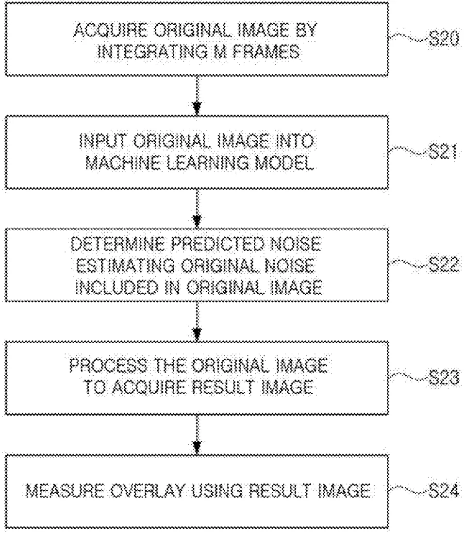
Samsung describes a method that uses a machine learning model to remove noise from images taken by a scanning electron microscope. The system trains the model to identify and predict noise patterns, allowing it to produce clearer images from fewer data frames than previously required.
In the filing’s own words
A method of measuring an overlay includes obtaining a plurality of first images, each of the plurality of first images being generated by integrating N first frames generated by a scanning electron microscope (SEM) device, generating a plurality of training images by respectively applying noise to the plurality of first images, inputting the plurality of training images into a machine learning model, obtaining, from the machine learning model, predicted noise by determining, by the machine learning model, noise in each of the plurality of training images, training the machine learning model by respectively comparing the predicted noise of the plurality of training images with the noise applied to the plurality of first images, obtaining an original image in which M second frames generated by the SEM device are integrated, obtaining a result image by inputting the original image into the machine learning model for which training is completed.
What exactly they claim (claim 1)
1. A method of measuring an overlay, comprising: obtaining a plurality of first images, each of the plurality of first images being generated by integrating N first frames generated by a scanning electron microscope (SEM) device, wherein Nis a natural number equal to or greater than 2; generating a plurality of training images by respectively applying noise to the plurality of first images; inputting the plurality of training images into a machine learning model; obtaining, from the machine learning model, predicted noise by determining, by the machine learning model, noise in each of the plurality of training images; training the machine learning model by respectively comparing the predicted noise of the plurality of training images with the noise applied to the plurality of first images; obtaining an original image in which M second frames generated by the SEM device are integrated, wherein M is a natural number less than N; obtaining a result image by inputting the original image into the machine learning model for which training is completed; and measuring an overlay based on the result image.
Facts
- Company
- Samsung (SAMSUNG ELECTRONICS CO., LTD.)
- Official title
- METHOD FOR MEASURING OVERLAY USING SCANNING ELECTRON MICROSCOPE DEVICE
- Publication number
- US20260301156A1
- Application number
- 19353945
- Filed
- Oct 9, 2025
- Published
- Oct 1, 2026
- Inventors
- 9
- Claims
- 20
Classified under
G06T 7/001 Physics & computingG06T 7/60 Physics & computingG06T 7/74 Physics & computingH01J 37/222 Electricity & electronicsG06T 2207/10061 Physics & computingG06T 2207/20081 Physics & computingMore from Samsung in AI & software
- Samsung patents tool to erase objects from photos using AI Sep 24, 2026
- Samsung patents drawing objects into photos with AI Oct 15, 2026
- Samsung patents AI that creates personalized exercise videos Sep 10, 2026
- Samsung patents AI summaries for paused TV shows based on your viewing habits Sep 24, 2026
- Samsung patents turning chat conversations into image prompts Oct 1, 2026
Summaries are simplified from the filing’s own abstract and first claim. A patent filing is not a product announcement.
Patent data and drawings: U.S. Patent and Trademark Office (USPTO). Nebula is not affiliated with or endorsed by the USPTO.