Sony patents LCD design that keeps liquid crystal from degrading
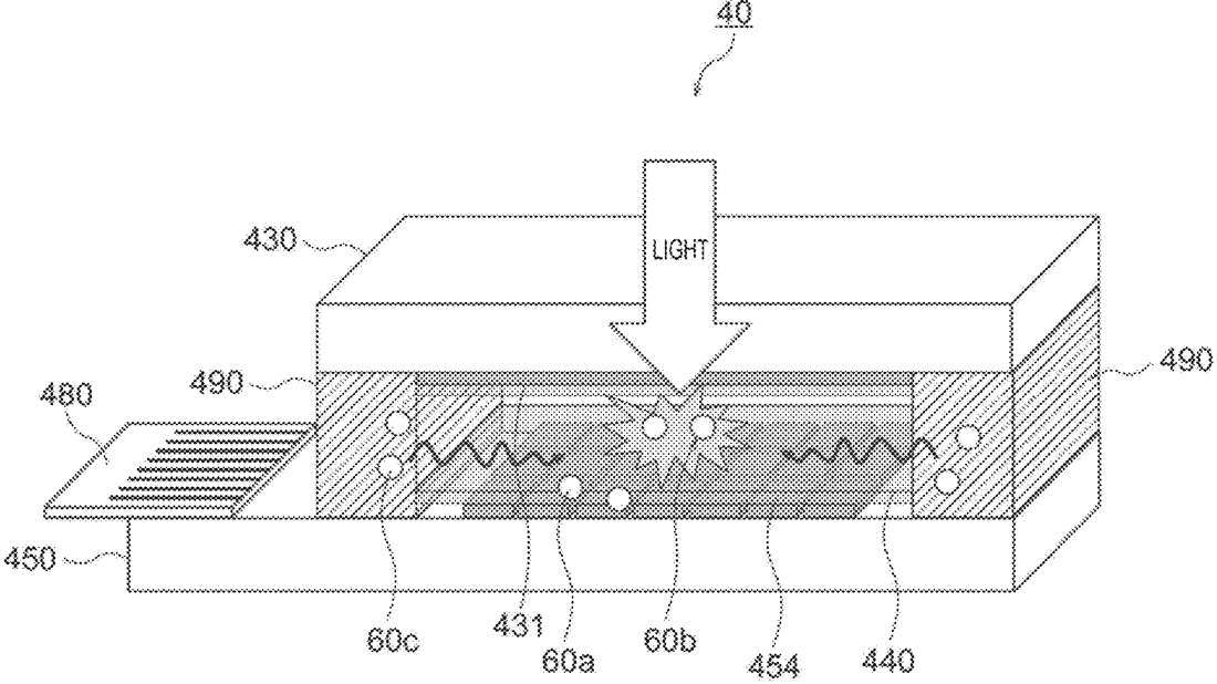
Sony describes a liquid crystal display structure where protective films cover the alignment layers in the main viewing area. In the border area outside the pixels, one of these alignment layers is left exposed to touch the liquid crystal directly. This setup is designed to help maintain the display's performance over time.
In the filing’s own words
To provide a liquid crystal display device capable of suppressing deterioration of display characteristics. A liquid crystal display device according to the present disclosure includes a first electrode provided in an effective pixel region in which pixels are arranged in a two-dimensional array, a second electrode opposed to the first electrode in a first direction, a liquid crystal provided between the first electrode and the second electrode, a first protective film and a second protective film opposed to each other in the first direction with the liquid crystal sandwiched between the first protective film and the second protective film in the effective pixel region, a first alignment film covered with the first protective film in the effective pixel region, a second alignment film covered with the second protective film in the effective pixel region, and a third electrode opposed to the second electrode in the first direction in a non-effective region located outside the effective pixel region. At least one of the first alignment film and the second alignment film is exposed in the non-effective region and is in contact with the liquid crystal.
What exactly they claim (claim 1)
1. A liquid crystal display device comprising: a first electrode provided in an effective pixel region in which pixels are arranged in a two-dimensional array; a second electrode opposed to the first electrode in a first direction; a liquid crystal provided between the first electrode and the second electrode; a first protective film and a second protective film opposed to each other in the first direction with the liquid crystal sandwiched between the first protective film and the second protective film in the effective pixel region; a first alignment film covered with the first protective film in the effective pixel region; a second alignment film covered with the second protective film in the effective pixel region; and a third electrode opposed to the second electrode in the first direction in a non-effective region located outside the effective pixel region, wherein at least one of the first alignment film and the second alignment film is exposed in the non-effective region and is in contact with the liquid crystal.
Facts
- Company
- Sony (SONY SEMICONDUCTOR SOLUTIONS CORPORATION)
- Official title
- LIQUID CRYSTAL DISPLAY DEVICE AND ELECTRONIC APPARATUS
- Publication number
- US20260299358A1
- Application number
- 19479519
- Filed
- Apr 10, 2024
- Published
- Oct 1, 2026
- Inventors
- 1
- Claims
- 20
Classified under
G02F 1/134336 Physics & computingG02F 1/133707 Physics & computingG02F 1/1339 Physics & computingG03B 21/006 Physics & computingMore from Sony in Chips & hardware
- Sony patents light sensor that adjusts how it counts incoming photons Sep 1, 2026
- Sony patents camera sensor with two pixel types for better motion detection Sep 1, 2026
- Sony patents game graphics that adjust quality based on hardware heat Sep 8, 2026
- Sony patents camera sensor design that stacks chips to shrink pixels Sep 8, 2026
- Sony patents chip design that measures internal temperature from outside Sep 8, 2026
Summaries are simplified from the filing’s own abstract and first claim. A patent filing is not a product announcement.
Patent data and drawings: U.S. Patent and Trademark Office (USPTO). Nebula is not affiliated with or endorsed by the USPTO.