Sony patents stacked chip design to fit more transistors in less space
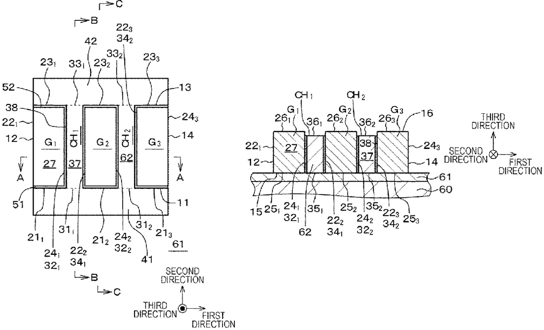
Sony describes a semiconductor structure where gate electrodes and channel regions are stacked in alternating layers on a base. This vertical arrangement allows multiple transistors to be built in a compact footprint rather than spreading them out horizontally.
In the filing’s own words
A semiconductor device including a structure having N gate electrode layers G and (N−1) channel formation region layers CH (where N≥3) alternately juxtaposed on an insulating material layer of a base having the insulating material layer formed on a surface of a conductive substrate. Each of the structure, the channel formation region layer CH, and the gate electrode layer G has a bottom surface, a top surface, and four side surfaces. A second surface of the nth channel formation region layer is connected to a fourth surface of the nth gate electrode layer. A fourth surface of the nth channel formation region layer is connected to a second surface of the (n+1)th gate electrode layer. One of an odd-numbered layer of the gate electrode layers and an even-numbered layer of the gate electrode layers is connected to a first contact portion and the other is connected to a second contact portion.
What exactly they claim (claim 1)
1. A semiconductor device, comprising: a conductive substrate; an insulating material layer, wherein a first surface of the insulating material layer is in contact with and is disposed on a surface of the conductive substrate; a plurality of gate electrode layers, wherein each gate electrode layer in the plurality of gate electrode layers is disposed on a second surface of the insulating material layer, and wherein the second surface of the insulating material layer is opposite the first surface of the insulating material layer; a plurality of channel formation region layers, wherein each channel formation region layer in the plurality of channel formation region layers is disposed on the second surface of the insulating material layer, wherein each channel formation region layer in the plurality of channel formation region layers is disposed between a unique pair of gate electrode layers of the plurality of gate electrode layers; a first source/drain region, wherein the first source/drain region is disposed on the second surface of the insulating material layer, wherein the first source/drain region is in contact with a first side surface of each of the channel formation region layers in the plurality of channel formation region layers; a second source/drain region, wherein the second source/drain region is disposed on the second surface of the insulation material layer, wherein the second source/drain region is in contact with a second side surface of each of the channel formation region layers in the plurality of channel formation region layers, and wherein the first side surface of the channel formation region layers is opposite the second side surface of the channel formation region layers; a first insulating film, wherein the first insulating film is disposed on first side surfaces of each of the gate electrode layers in the plurality of gate electrode layers, and wherein the first insulating film lies between the first side surfaces of each of the gate electrode layers in the plurality of gate electrode layers and the first source/drain region; and a second insulating film, wherein the second insulating film is disposed on second side surfaces of each of the gate electrode layers in the plurality of gate electrode layers, wherein the second insulating film lies between the second side surfaces of each of the gate electrode layers in the plurality of gate electrode layers and the second source/drain region, wherein a bottom surface of each gate electrode layer in the plurality of gate electrode layers is in direct contact with the insulating material layer, wherein the first insulating film and the second insulating film include are formed from an insulating portion, and wherein the insulating portion is in direct contact with first, second, third, and fourth side surfaces of at least one gate electrode layer in the plurality of gate electrode layers.
Facts
- Company
- Sony (SONY SEMICONDUCTOR SOLUTIONS CORPORATION)
- Official title
- Semiconductor device
- Patent number
- US12772479B2
- Application number
- 18379993
- Filed
- Oct 13, 2023
- Granted
- Oct 20, 2026
- Inventors
- 2
- Claims
- 15
Classified under
H10D 30/031 Electricity & electronicsH10D 30/6755 Electricity & electronicsMore from Sony in Chips & hardware
- Sony patents light sensor that adjusts how it counts incoming photons Sep 1, 2026
- Sony patents camera sensor with two pixel types for better motion detection Sep 1, 2026
- Sony patents game graphics that adjust quality based on hardware heat Sep 8, 2026
- Sony patents camera sensor design that stacks chips to shrink pixels Sep 8, 2026
- Sony patents chip design that measures internal temperature from outside Sep 8, 2026
Summaries are simplified from the filing’s own abstract and first claim. A patent filing is not a product announcement.
Patent data and drawings: U.S. Patent and Trademark Office (USPTO). Nebula is not affiliated with or endorsed by the USPTO.