Nvidia patents memory setup that matches data speed to processor needs
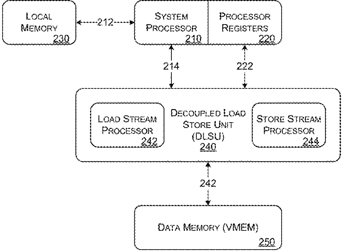
This patent describes a system that adjusts how fast data moves between a processor and memory based on their individual speeds. It uses a separate unit to preload data into a buffer, ensuring the processor does not have to wait for information to arrive.
In the filing’s own words
Aspects of this technical solution can provide at least a technical improvement to reading and writing data between a memory device and a processor, including, for example, by providing a technical solution to configure one or more load streams with stream sizes configured based on relative speed of a processor and a memory. For example, this technical solution can provide a technical improvement to processing speed of computations by a processor with data obtained from or stored to a memory device. For example, a system in accordance with this technical solution can provide a decoupled load store unit (DLSU) distinct from a processor and a memory device to prefetch a sufficient amount of data from a memory device into a stream buffer of a DLSU, to provide instructions to a processor at a rate that eliminates waiting by the processor for memory over one or more cycles.
What exactly they claim (claim 1)
1. A system, comprising: a memory device; a first processor including a stream processor and a scheduling processor, the first processor coupled with the memory device; a second processor coupled with the first processor; one or more processors to: configure, according to a first latency of the memory device, the stream processor to read from or write to the memory device at the first latency; configure, according to a second latency of the second processor, the scheduling processor to read from or write to with one or more memory registers of the second processor at the second latency; provide data between the first processor and the memory device at the first latency; and provide data between the second processor and the stream processor at the second latency.
Facts
- Company
- Nvidia (NVIDIA Corporation)
- Official title
- Memory architecture
- Patent number
- US12769677B2
- Application number
- 18789896
- Filed
- Jul 31, 2024
- Granted
- Oct 20, 2026
- Inventors
- 6
- Claims
- 20
Classified under
G06F 13/1689 Physics & computingG06F 9/30043 Physics & computingG06F 13/1673 Physics & computingMore from Nvidia in Chips & hardware
- Nvidia patents method to skip zero data in neural network math Oct 13, 2026
- Nvidia patents hardware to speed up motion blur in ray tracing Oct 13, 2026
- Nvidia patents method to sync data across split processor chips Sep 17, 2026
- Nvidia patents chip math trick to speed up AI calculations Oct 8, 2026
- Nvidia patents data center cooling that uses cryogenic fluids Oct 15, 2026
Summaries are simplified from the filing’s own abstract and first claim. A patent filing is not a product announcement.
Patent data and drawings: U.S. Patent and Trademark Office (USPTO). Nebula is not affiliated with or endorsed by the USPTO.