Nvidia patents method to pinpoint heat failures in chip layers
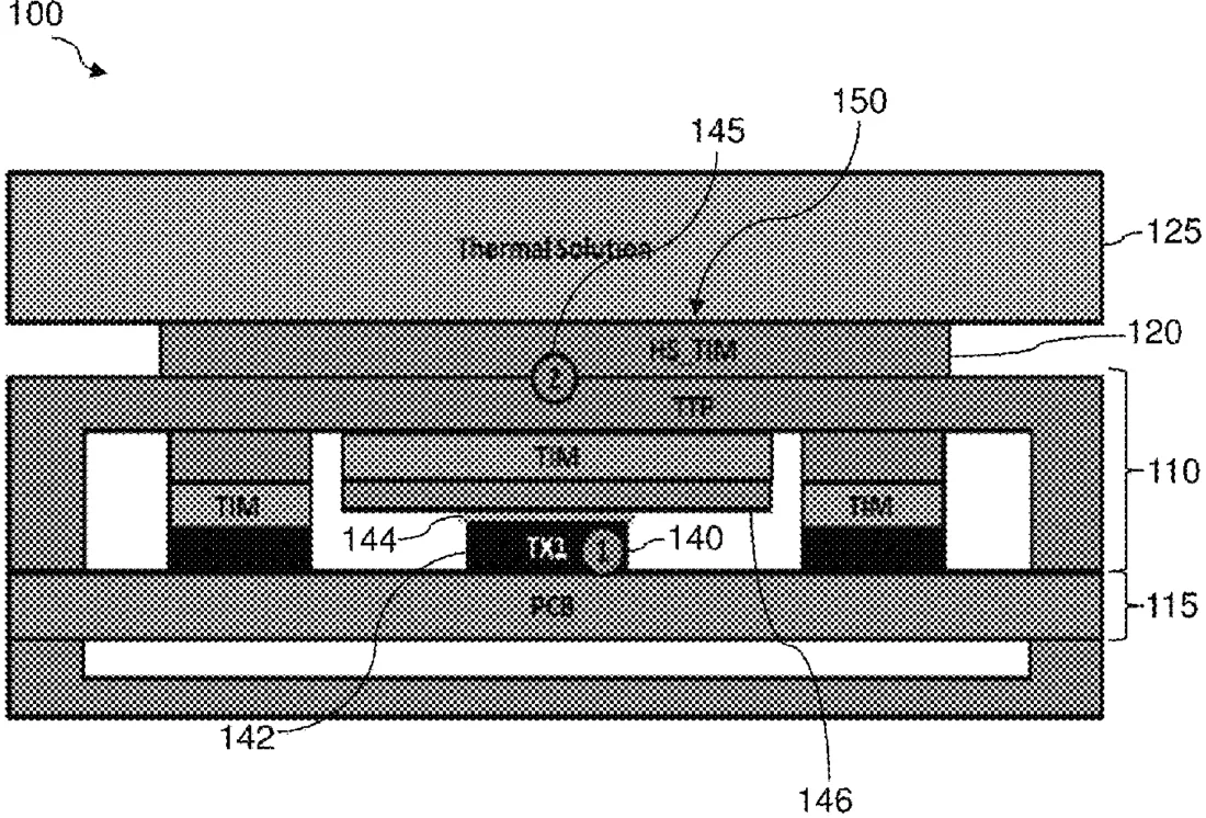
Nvidia describes a testing method that identifies exactly which layer of a chip package is causing heat problems. It compares measured thermal data against known good values to isolate specific failures. This allows manufacturers to sort chips into groups for repair or discard based on the specific layer that failed.
In the filing’s own words
Testing chip or board packages for thermal failure can be conducted at various stages of the package's life cycle. Conventional testing can detect a thermal failure of the package, though conventional testing does not detect at which specific thermal layer a failure has occurred. By applying an R deviation percentage to the measured thermal parameters received from a testing unit, a specific breakdown of each thermal interface layer can be analyzed. Each thermal interface layer has an associated gold value which is a known good value of thermal energy at a specific time interval. The gold value can be compared to the timing results calculated from the measured thermal parameters. This comparison can then identify which thermal interface layers, if any, are causing the thermal failure of the package. The thermal interface layer can then be repaired or the manufacturing process can be modified to eliminate the failure.
What exactly they claim (claim 1)
1. A method, comprising: determining an R deviation percentage threshold for each thermal interface layer in a set of thermal interface layers, wherein the set of thermal interface layers is part of a chip package or a board package undergoing a thermal test; calculating an R deviation for each thermal interface layer in the set of thermal interface layers using the R deviation percentage threshold, wherein the R deviation is an integral of the change in power over a time interval; obtaining thermal measurements from a testing jig that supplies power to the chip package or the board package and measures thermal characteristics over a time interval; determining a measured time parameter from the R deviation and the thermal measurements from the chip package or the board package for each thermal interface layer in the set of thermal interface layers; identifying at least one thermal failure parameter for at least one thermal interface layer in the set of thermal interface layers by comparing the measured time parameter to a thermal interface layer gold value for each respective thermal interface layer; and moving, by a package sorter using the at least one thermal failure parameter, the chip package or the board package to a designated place, wherein the chip package or the board package that passes each thermal interface layer test is placed in a first group, the chip package or the board package that fails at least one thermal interface layer test and is repairable is placed in a second group, and the chip package or the board package that fails at least one thermal interface layer test and is not repairable is placed in a third group.
Facts
- Company
- Nvidia (NVIDIA Corporation)
- Official title
- Thermal measurement for complex thermal stack up products
- Patent number
- US12768879B2
- Application number
- 18734859
- Filed
- Jun 5, 2024
- Granted
- Oct 20, 2026
- Inventors
- 2
- Claims
- 20
Classified under
G01R 31/2874 Physics & computingG01R 31/2889 Physics & computingG01R 31/2891 Physics & computingMore from Nvidia in Chips & hardware
- Nvidia patents method to skip zero data in neural network math Oct 13, 2026
- Nvidia patents hardware to speed up motion blur in ray tracing Oct 13, 2026
- Nvidia patents method to sync data across split processor chips Sep 17, 2026
- Nvidia patents chip math trick to speed up AI calculations Oct 8, 2026
- Nvidia patents data center cooling that uses cryogenic fluids Oct 15, 2026
Summaries are simplified from the filing’s own abstract and first claim. A patent filing is not a product announcement.
Patent data and drawings: U.S. Patent and Trademark Office (USPTO). Nebula is not affiliated with or endorsed by the USPTO.