Sony patents smaller sensor package using built-in cooling element
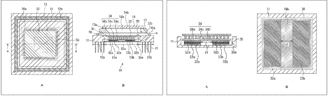
Sony describes a design for a semiconductor package that fits a sensor chip into a recessed area of the housing. A Peltier element, a device that moves heat from one side to the other, is placed between the chip and the package to manage temperature. The components are connected using a conductive resin to link electrical terminals across the gap.
In the filing’s own words
The present technology relates to a semiconductor apparatus that makes it possible to make a sensor-chip package smaller in size, where a Peltier element is arranged in the sensor-chip package. The semiconductor apparatus includes a package that includes a concave portion; a sensor chip that is arranged in the concave portion; and a Peltier element that is arranged between the sensor chip and the package. A back-surface terminal and an upper-surface terminal are electrically connected to each other through a conductive resin, the back-surface terminal being formed on a back surface of a lower substrate of the Peltier element, the upper-surface terminal being formed on an upper surface of the concave portion to face the back-surface terminal. The present technology is applicable to, for example, a semiconductor apparatus that includes a built-in SWIR image sensor.
What exactly they claim (claim 1)
1. A semiconductor apparatus, comprising: a package that includes a concave portion; a sensor chip that is arranged in the concave portion; and a Peltier element that is arranged between the sensor chip and the package, wherein a back-surface terminal and an upper-surface terminal are electrically connected to each other through a conductive resin, the back-surface terminal being formed on a back surface of a lower substrate of the Peltier element, the upper-surface terminal being formed on an upper surface of the concave portion to face the back-surface terminal.
Facts
- Company
- Sony (SONY SEMICONDUCTOR SOLUTIONS CORPORATION)
- Official title
- Semiconductor apparatus
- Patent number
- US12765378B2
- Application number
- 18717571
- Filed
- Dec 1, 2022
- Granted
- Oct 13, 2026
- Inventors
- 4
- Claims
- 31
Classified under
H10W 40/28 Electricity & electronicsH10F 39/804 Electricity & electronicsH10F 39/811 Electricity & electronicsMore from Sony in Chips & hardware
- Sony patents light sensor that adjusts how it counts incoming photons Sep 1, 2026
- Sony patents camera sensor with two pixel types for better motion detection Sep 1, 2026
- Sony patents game graphics that adjust quality based on hardware heat Sep 8, 2026
- Sony patents camera sensor design that stacks chips to shrink pixels Sep 8, 2026
- Sony patents chip design that measures internal temperature from outside Sep 8, 2026
Summaries are simplified from the filing’s own abstract and first claim. A patent filing is not a product announcement.
Patent data and drawings: U.S. Patent and Trademark Office (USPTO). Nebula is not affiliated with or endorsed by the USPTO.