Sony patents chip design with direct heat paths for better reliability
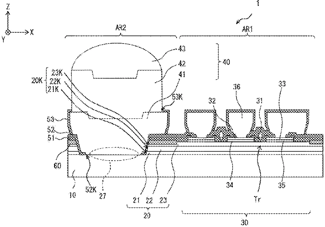
Sony describes a semiconductor device that improves heat management by creating a direct path for heat to escape. The design includes a specific layer with holes that allow a high-conductivity heat dissipation unit to touch the base substrate, bypassing insulating layers. This structure helps keep transistors cooler and more reliable during operation.
In the filing’s own words
Provided is a semiconductor device having high heat dissipation and high operation reliability. This semiconductor device includes a semiconductor substrate, a first semiconductor layer that is provided on the semiconductor substrate, has a first aperture, and has a first thermal conductivity, a transistor (Tr) provided on the first semiconductor layer, and a heat dissipation unit that is in contact with the semiconductor substrate via the first aperture and has a second thermal conductivity higher than the first thermal conductivity.
What exactly they claim (claim 1)
1. A semiconductor device, comprising: a semiconductor substrate; a first semiconductor layer on the semiconductor substrate, wherein the first semiconductor layer has a first aperture, and a first thermal conductivity; a transistor on the first semiconductor layer; a heat dissipation unit in contact with the semiconductor substrate via the first aperture, wherein the heat dissipation unit has a second thermal conductivity higher than the first thermal conductivity; and a plurality of transistors, wherein the plurality of transistors include the transistor, the plurality of transistors is arranged to be adjacent to each other in a first direction, each of the plurality of transistors includes a gate electrode that extends in a second direction perpendicular to the first direction, and the plurality of transistors satisfies a following condition expression (A): ( L 2/ L 1)≤2 (A) where L1 is a length of the gate electrode of each of the plurality of transistors in the second direction, and L2 is a distance in the second direction between a center position of the heat dissipation unit in the second direction and a center position of the gate electrode of each of the plurality of transistors in the second direction.
Facts
- Company
- Sony (SONY SEMICONDUCTOR SOLUTIONS CORPORATION)
- Official title
- Semiconductor device, semiconductor module, and wireless communication apparatus
- Patent number
- US12764991B2
- Application number
- 18579634
- Filed
- Mar 18, 2022
- Granted
- Oct 13, 2026
- Inventors
- 2
- Claims
- 12
Classified under
H10D 30/475 Electricity & electronicsH10D 30/015 Electricity & electronicsH10D 62/824 Electricity & electronicsH10D 84/82 Electricity & electronicsH10W 40/10 Electricity & electronicsH10D 62/8503 Electricity & electronicsMore from Sony in Chips & hardware
- Sony patents light sensor that adjusts how it counts incoming photons Sep 1, 2026
- Sony patents camera sensor with two pixel types for better motion detection Sep 1, 2026
- Sony patents game graphics that adjust quality based on hardware heat Sep 8, 2026
- Sony patents camera sensor design that stacks chips to shrink pixels Sep 8, 2026
- Sony patents chip design that measures internal temperature from outside Sep 8, 2026
Summaries are simplified from the filing’s own abstract and first claim. A patent filing is not a product announcement.
Patent data and drawings: U.S. Patent and Trademark Office (USPTO). Nebula is not affiliated with or endorsed by the USPTO.