Sony patents camera sensor design to reduce noise in tiny transistors
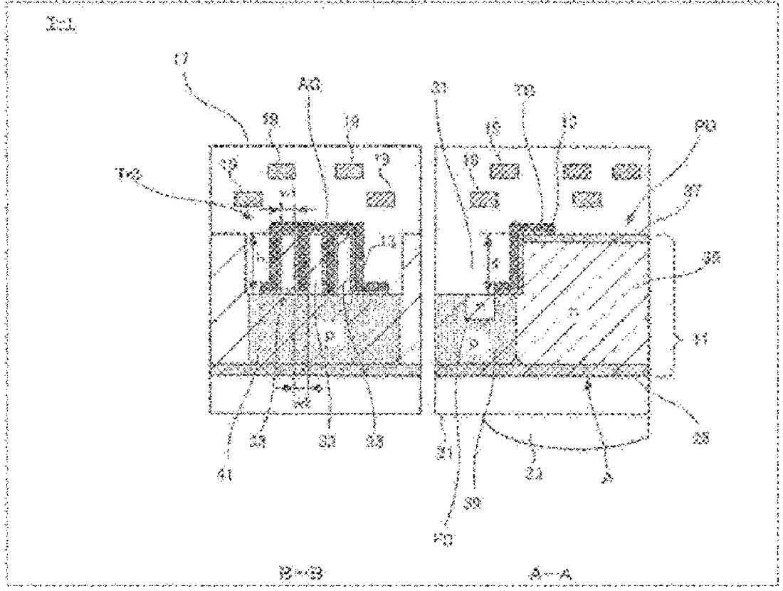
Sony has secured a patent for a solid-state imaging device, commonly found in camera sensors, that uses a specific type of amplifying transistor to handle electrical signals. The design features a fully-depleted transistor structure intended to manage the flow of charge from the light-sensitive parts of the sensor. This approach aims to maintain signal quality even as the physical components of the sensor become smaller.
In the filing’s own words
The present technique relates to a solid-state imaging device, a solid-state imaging device manufacturing method, and an electronic apparatus that are capable of providing a solid-state imaging device that can prevent generation of RTS noise due to miniaturization of amplifying transistors, and can achieve a smaller size and a higher degree of integration accordingly. A solid-state imaging device includes a photodiode as a photoelectric conversion unit, a transfer gate that reads out charges from the photodiode, a floating diffusion from which the charges of the photodiode are read by an operation of the transfer gate, and an amplifying transistor connected to the floating diffusion. More particularly, the amplifying transistor is of a fully-depleted type. Such an amplifying transistor includes an amplifier gate (gate electrode) extending in a direction perpendicular to convex strips formed by processing a surface layer of a semiconductor layer, for example.
What exactly they claim (claim 1)
1. A light detecting device, comprising: a first photoelectric conversion unit; a transfer gate configured to read out charges from the first photoelectric conversion unit; a floating diffusion from which the charges of the first photoelectric conversion unit are read by an operation of the transfer gate; and an amplifying transistor connected to the floating diffusion, wherein a channel portion of the amplifying transistor comprises an intrinsic semiconductor.
Facts
- Company
- Sony (SONY SEMICONDUCTOR SOLUTIONS CORPORATION)
- Official title
- Solid-state imaging device, method of manufacturing solid-state imaging device, and electronic apparatus
- Patent number
- US12764436B2
- Application number
- 18804704
- Filed
- Aug 14, 2024
- Granted
- Oct 13, 2026
- Inventors
- 1
- Claims
- 8
Classified under
H04N 25/76 Electricity & electronicsH04N 25/618 Electricity & electronicsH04N 25/77 Electricity & electronicsH04N 25/78 Electricity & electronicsH10F 39/18 Electricity & electronicsH10F 39/8027 Electricity & electronicsMore from Sony in Chips & hardware
- Sony patents light sensor that adjusts how it counts incoming photons Sep 1, 2026
- Sony patents camera sensor with two pixel types for better motion detection Sep 1, 2026
- Sony patents game graphics that adjust quality based on hardware heat Sep 8, 2026
- Sony patents camera sensor design that stacks chips to shrink pixels Sep 8, 2026
- Sony patents chip design that measures internal temperature from outside Sep 8, 2026
Summaries are simplified from the filing’s own abstract and first claim. A patent filing is not a product announcement.
Patent data and drawings: U.S. Patent and Trademark Office (USPTO). Nebula is not affiliated with or endorsed by the USPTO.