Sony patents camera chip that adjusts processing speed to save power
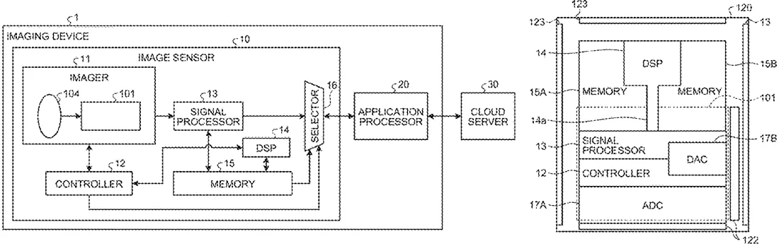
Sony has patented a camera sensor design that uses a neural network to analyze images and switch between two processing speeds. The chip arranges its components in a specific order to reduce power usage while the system decides how fast to process each frame.
In the filing’s own words
A solid-state imaging device includes an imager that acquires image data, a processing unit that performs a process based on a neural network calculation model for data based on the image data acquired from the imager, and a control unit that switches between a first process mode of performing a first process at a first frame rate and, based on a result of the first process, a second process mode of performing a second process at a second frame rate.
What exactly they claim (claim 1)
1. A solid-state imaging device, comprising: an imager configured to output image data; processing circuitry configured to execute, in a first process mode, a first process using a neural network calculation model based on the outputted image data; a pixel array; an analog-to-digital converter (ADC); a signal processor, wherein the ADC, the signal processor, and the processing circuitry are arranged in a layout in order from an upstream side along a flow of a signal read out from the pixel array, wherein the layout reduces power consumption; and a controller configured to: readout the image data from the imager based on a selection of the first process mode; start the first process for the readout image data with the neural network calculation model after the readout of the image data from the imager is completed; switch between the first process mode and a second process mode based on a result of the first process; and control execution of a second process that corresponds to the second process mode.
Facts
- Company
- Sony (Sony Semiconductor Solutions Corporation)
- Official title
- Solid-state imaging device and electronic device
- Patent number
- US12756947B2
- Application number
- 18963804
- Filed
- Nov 29, 2024
- Granted
- Oct 6, 2026
- Inventors
- 1
- Claims
- 13
Classified under
H04N 25/46 Electricity & electronicsH04N 23/61 Electricity & electronicsH04N 25/40 Electricity & electronicsH04N 25/41 Electricity & electronicsH04N 25/50 Electricity & electronicsH04N 25/78 Electricity & electronicsMore from Sony in Chips & hardware
- Sony patents light sensor that adjusts how it counts incoming photons Sep 1, 2026
- Sony patents camera sensor with two pixel types for better motion detection Sep 1, 2026
- Sony patents game graphics that adjust quality based on hardware heat Sep 8, 2026
- Sony patents camera sensor design that stacks chips to shrink pixels Sep 8, 2026
- Sony patents chip design that measures internal temperature from outside Sep 8, 2026
Summaries are simplified from the filing’s own abstract and first claim. A patent filing is not a product announcement.
Patent data and drawings: U.S. Patent and Trademark Office (USPTO). Nebula is not affiliated with or endorsed by the USPTO.