Samsung patents watch design that fits charging coil around sensor
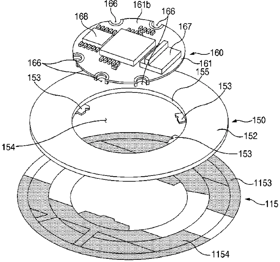
Samsung has been granted a patent for a wearable device layout that places an optical sensor module directly inside the opening of a wireless charging coil. This arrangement allows the sensor's circuit board to sit within the coil's center, connecting to the main processor while sharing the same physical space. The design uses specific connectors to link the sensor and charging components without adding extra layers.
In the filing’s own words
An electronic device is disclosed, including a rear cover; a first circuit; and a module assembly disposed between the first circuit board and the rear cover, wherein the module assembly includes an optical sensor module including a second circuit board electrically connected with the first circuit board via a first connector, and a wireless charging module including a charging coil and electrically connected with the second circuit board, wherein the wireless charging module is disposed in proximity of the optical sensor module such that the second circuit board is substantially surrounded by the charging coil, and that, when viewed in a direction from a side of the wearable device, the second circuit board is located between a first geometric plane extending a first face of the wireless charging module and a second geometric plane extending a second face of the wireless charging module.
What exactly they claim (claim 1)
1. A wearable device comprising: a rear cover; a first circuit board including a processor disposed thereon; and a module assembly disposed between the first circuit board and the rear cover, the module assembly including: an optical sensor module including a second circuit board including a first surface facing the rear cover and a second surface opposite to the first surface, a light emitter, and a light receiver, the second circuit board electrically connected with the first circuit board via a first connection member disposed on the second surface of the second circuit board, each of the light emitter and light receiver disposed on the first surface of the second circuit board; and a wireless charging module including a charging coil physically coupled to the second circuit board via a second connection member, when viewed in a direction from a side of the wearable device, the second circuit board located substantially a same plane as the wireless charging module, wherein the wireless charging module is disposed in proximity of the optical sensor module such that the second circuit board is located in an opening area substantially surrounded by the charging coil, and wherein a portion of the first connection member is accommodated within the opening area.
Facts
- Company
- Samsung (Samsung Electronics Co., Ltd.)
- Official title
- Wearable electronic device including module assembly comprising an optical sensor and wireless charging
- Patent number
- US12748387B2
- Application number
- 18624262
- Filed
- Apr 2, 2024
- Granted
- Sep 29, 2026
- Inventors
- 6
- Claims
- 20
Classified under
G04G 19/00 Physics & computingG04G 9/007 Physics & computingG04G 21/025 Physics & computingH02J 7/70 Electricity & electronicsH02J 50/005 Electricity & electronicsH05K 1/028 Electricity & electronicsMore from Samsung in Wearables
- Samsung patents wearable that tracks brain waves to suggest health actions Oct 6, 2026
- Samsung patents wristwatch with flexible screen that wraps around your wrist Oct 15, 2026
- Samsung patents ring that projects a screen onto your skin Oct 22, 2026
- Samsung patents glasses with moving lenses to adjust focus Sep 1, 2026
- Samsung patents wearable that adjusts walking force while you test walk Sep 8, 2026
Summaries are simplified from the filing’s own abstract and first claim. A patent filing is not a product announcement.
Patent data and drawings: U.S. Patent and Trademark Office (USPTO). Nebula is not affiliated with or endorsed by the USPTO.