Sony patents camera sensor design that reduces wiring complexity
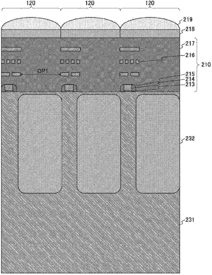
Sony describes an imaging device that uses switches to combine signals from different columns of pixels. This design allows the sensor to process data in groups, or 'bin,' without needing extra wires for each individual pixel column.
In the filing’s own words
Binning is enabled while suppressing an increase in the number of switches connected to a signal line that transmits signals read out from pixels in a column direction. An imaging device includes a pixel array unit in which pixels are arranged in a matrix in a row direction and a column direction; a signal line that transmits signals read out from the pixels in the column direction; a sample-and-hold switch that samples and holds the signals, which are transmitted via the signal line, for each column; and a connection switch that connects signal lines of different columns in which the signals are sampled and held. The imaging device may further include an AD conversion unit that performs AD conversion for each of the columns of the signals transmitted via the signal lines; and an active control unit that activates one AD conversion unit out of the AD conversion units of each column connected via the connection switch.
What exactly they claim (claim 1)
1. An imaging device comprising: a pixel array unit in which pixels are arranged in a matrix in a row direction and a column direction; a signal line that transmits signals read out from the pixels in the column direction; a sample-and-hold switch that samples and holds the signals, which are transmitted via the signal line, for each column; and a connection switch that connects signal lines of different columns in which the signals are sampled and held.
Facts
- Company
- Sony (SONY SEMICONDUCTOR SOLUTIONS CORPORATION)
- Official title
- IMAGING DEVICE
- Publication number
- US20260332914A1
- Application number
- 19104355
- Filed
- Jun 30, 2023
- Published
- Oct 22, 2026
- Inventors
- 1
- Claims
- 20
Classified under
H04N 25/78 Electricity & electronicsH04N 25/46 Electricity & electronicsH04N 25/772 Electricity & electronicsMore from Sony in Cameras & imaging
- Sony patents camera chips that sign photos to prove they are real Sep 15, 2026
- Sony patents camera setup that learns to mimic a virtual view Sep 1, 2026
- Sony patents camera method to reduce lag in burst mode photos Sep 1, 2026
- Sony patents camera sensor design to improve global shutter image quality Sep 1, 2026
- Sony patents camera lens that subtracts light waves to cut data processing Sep 8, 2026
Summaries are simplified from the filing’s own abstract and first claim. A patent filing is not a product announcement.
Patent data and drawings: U.S. Patent and Trademark Office (USPTO). Nebula is not affiliated with or endorsed by the USPTO.