Sony patents camera sensor design to reduce noise in images
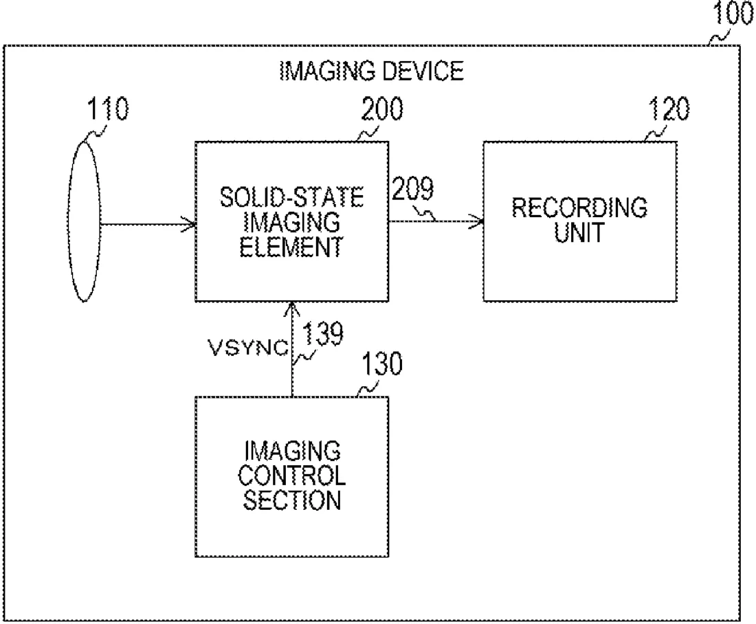
Sony describes a camera sensor design that uses two separate storage areas to hold image data. The sensor reads the data in a specific sequence to clean up the signal before it is processed.
In the filing’s own words
Solid-state imaging elements are disclosed. In one example, an upstream circuit sequentially generates a predetermined reset level and a signal level corresponding to an exposure amount, and causes first and second capacitive elements to hold the reset level and the signal level. A selection circuit sequentially connects one of the capacitive elements to a predetermined downstream node, disconnects both capacitive elements from the downstream node, and connects the other capacitive element to the downstream node. A downstream reset transistor initializes a level of the downstream node when both capacitive elements are disconnected from the downstream node. A downstream circuit sequentially reads the reset level and the signal level from the first and second capacitive elements via the downstream node and outputs the reset level and the signal level.
What exactly they claim (claim 1)
1. A solid-state imaging element comprising: a photoelectric conversion element that converts incident light into a charge; a floating diffusion configured to receive and store the charge; a transfer transistor having a first terminal coupled to the photoelectric conversion element and a second terminal coupled to the floating diffusion; a first transistor having a first terminal coupled to a voltage source and a second terminal coupled to the floating diffusion; a first amplification transistor having a gate coupled to the floating diffusion, a first terminal coupled to the voltage source, and a second terminal configured to output a voltage corresponding to the charge; a first capacitive element; a second capacitive element; a first selection transistor having a first end coupled to the first capacitive element and a second end coupled to a node; a second selection transistor having a first end coupled to the second capacitive element and a second end coupled to the node; a third selection transistor coupled between the second terminal of the first amplification transistor and the node; a second transistor having a source or a drain coupled to the node; a second amplification transistor having a gate coupled to the node and configured to output a pixel signal; and a fourth selection transistor having a first end coupled to an output of the second amplification transistor and a second end coupled to a signal line.
Facts
- Company
- Sony (Sony Semiconductor Solutions Corporation)
- Official title
- SOLID-STATE IMAGING ELEMENT
- Publication number
- US20260332907A1
- Application number
- 19709684
- Filed
- Jun 16, 2026
- Published
- Oct 22, 2026
- Inventors
- 2
- Claims
- 20
Classified under
H04N 25/77 Electricity & electronicsH04N 25/616 Electricity & electronicsH04N 25/65 Electricity & electronicsH04N 25/78 Electricity & electronicsH04N 25/79 Electricity & electronicsMore from Sony in Cameras & imaging
- Sony patents camera chips that sign photos to prove they are real Sep 15, 2026
- Sony patents camera setup that learns to mimic a virtual view Sep 1, 2026
- Sony patents camera method to reduce lag in burst mode photos Sep 1, 2026
- Sony patents camera sensor design to improve global shutter image quality Sep 1, 2026
- Sony patents camera lens that subtracts light waves to cut data processing Sep 8, 2026
Summaries are simplified from the filing’s own abstract and first claim. A patent filing is not a product announcement.
Patent data and drawings: U.S. Patent and Trademark Office (USPTO). Nebula is not affiliated with or endorsed by the USPTO.