Samsung patents image sensor with separate reset lines for better photo quality
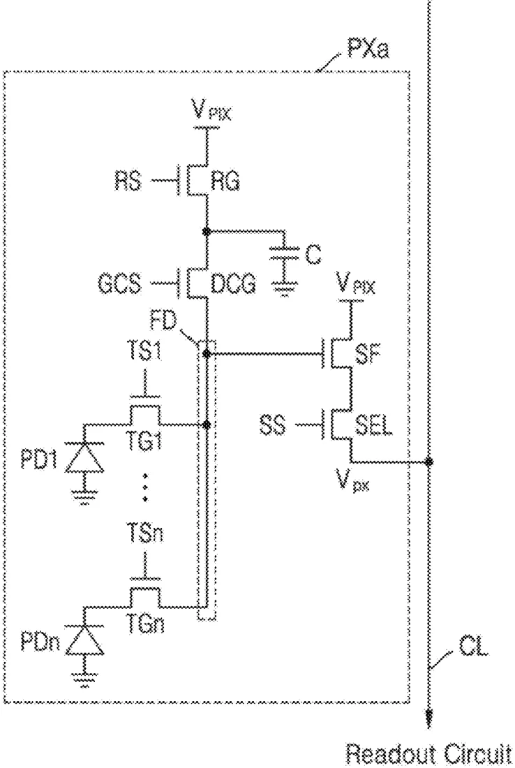
Samsung describes an image sensor design where each pixel contains two light detectors and a specific circuit setup. The key feature is a row driver that sends separate reset signals to individual pixels in the same row, allowing for more precise control over how the sensor clears and reads data.
In the filing’s own words
An image sensor includes a pixel array including a first pixel and a second pixel in a same row. Each of the first pixel and the second pixel includes a first photodiode and a second photodiode, a floating diffusion region (FD) electrically connected to the first and the second photodiodes, a capacitor electrically connected to the FD, a dual conversion gain transistor connected between the FD and the capacitor, and a reset transistor configured to provide a power supply voltage to the FD and the capacitor, and a row driver configured to provide a first reset control signal to a first reset transistor of the first pixel through a first row line of row lines, and provide a second reset control signal to a second reset transistor of the second pixel through a second row line of the row lines.
What exactly they claim (claim 1)
1. An image sensor comprising: a pixel array including a first pixel and a second pixel, the first pixel and the second pixel being in a same row, wherein each of the first pixel and the second pixel comprises, a first photodiode and a second photodiode; a floating diffusion region electrically connected to the first photodiode and the second photodiode; a capacitor electrically connected to the floating diffusion region; a dual conversion gain transistor connected between the floating diffusion region and the capacitor; and a reset transistor configured to provide a power supply voltage to the floating diffusion region and the capacitor, and a row driver configured to provide a plurality of control signals to the first pixel and the second pixel through a plurality of row lines, provide a first reset control signal to a first reset transistor of the first pixel through a first row line of the plurality of row lines, and provide a second reset control signal to a second reset transistor of the second pixel through a second row line of the plurality of row lines.
Facts
- Company
- Samsung (Samsung Electronics Co., Ltd.)
- Official title
- IMAGE SENSOR AND OPERATING METHOD OF THE SAME
- Publication number
- US20260332906A1
- Application number
- 19648069
- Filed
- Apr 15, 2026
- Published
- Oct 22, 2026
- Inventors
- 1
- Claims
- 20
Classified under
H04N 25/704 Electricity & electronicsH04N 25/78 Electricity & electronicsMore from Samsung in Cameras & imaging
- Samsung patents syncing multiple cameras to record one video Sep 1, 2026
- Samsung patents camera system that auto-picks best lens for video Oct 13, 2026
- Samsung patents camera design that bends light to fit in thinner phones Oct 20, 2026
- Samsung patents camera feature that saves video clips around photos Sep 10, 2026
- Samsung patents image sensor that captures depth and bright scenes Sep 24, 2026
Summaries are simplified from the filing’s own abstract and first claim. A patent filing is not a product announcement.
Patent data and drawings: U.S. Patent and Trademark Office (USPTO). Nebula is not affiliated with or endorsed by the USPTO.