Samsung patents image sensor with adjustable anti-reflection layer
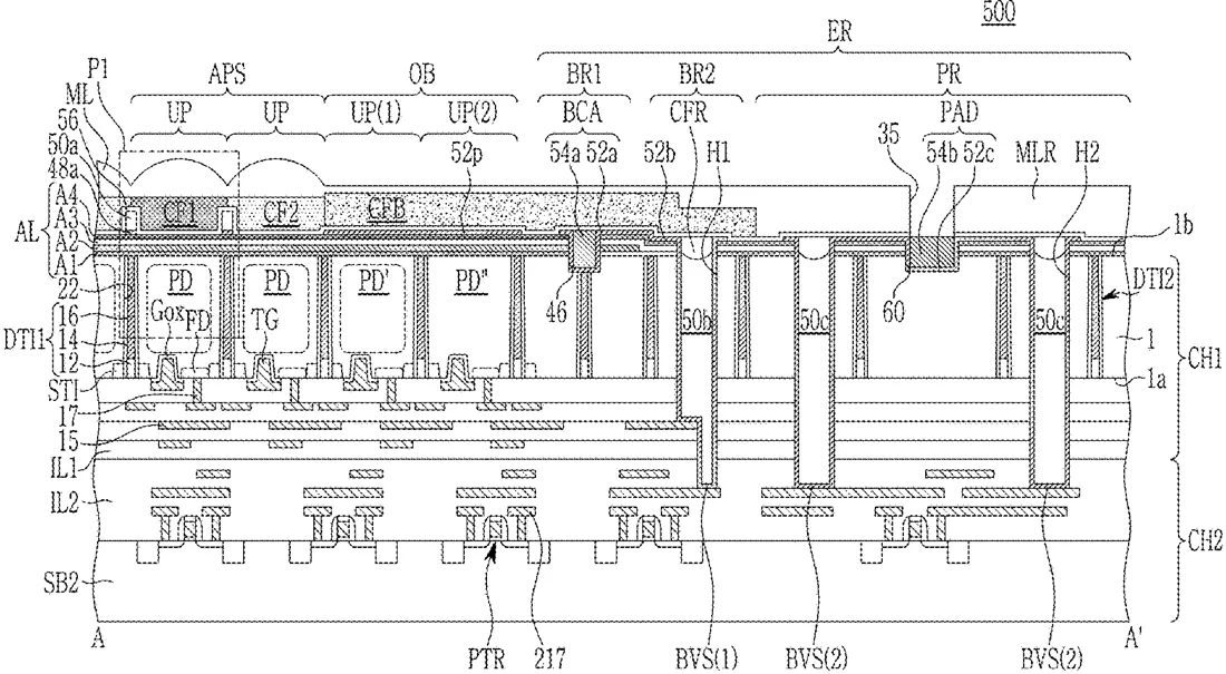
Samsung describes an image sensor design that places a conductive layer between insulating layers to reduce unwanted reflections. This layer covers the pixel area but avoids the edge sections where electrical connections are located, allowing voltage to be applied to control light behavior.
In the filing’s own words
Provided is an image sensor, which includes a first substrate that has a first surface and a second surface opposite to the first surface, and includes a pixel array area and an edge area, the edge area including a first conductive pad; an anti-reflection structure on the second surface; a pixel isolator in the first substrate and defining and separating pixels; and a micro lens array that is disposed on the anti-reflection structure, in which the anti-reflection structure includes a first insulating layer, a conductive layer, a second insulating layer, and a third insulating layer sequentially stacked, the conductive layer is on the pixel array area, and is not at least in a portion of the edge area where the first conductive pad is arranged, and a voltage is configured to be applied to the conductive layer.
What exactly they claim (claim 1)
1. An image sensor, comprising: a first substrate that has a first surface and a second surface opposite to the first surface, and includes a pixel array area and an edge area, the edge area including first conductive pad; an anti-reflection structure on the second surface; a pixel isolator in the first substrate defining and separating pixels; and a micro lens array on the anti-reflection structure, wherein the anti-reflection structure includes a first insulating layer and a conductive layer that are sequentially stacked, the conductive layer is on the pixel array area, and is not at least in a portion of the edge area where the first conductive pad is.
Facts
- Company
- Samsung (Samsung Electronics Co., Ltd.)
- Official title
- IMAGE SENSOR
- Publication number
- US20260324111A1
- Application number
- 19716594
- Filed
- Jun 23, 2026
- Published
- Oct 15, 2026
- Inventors
- 2
- Claims
- 20
Classified under
H10F 39/805 Electricity & electronicsG02B 1/116 Physics & computingH10F 39/024 Electricity & electronicsH10F 39/182 Electricity & electronicsH10F 39/8053 Electricity & electronicsH10F 39/8063 Electricity & electronicsMore from Samsung in Cameras & imaging
- Samsung patents syncing multiple cameras to record one video Sep 1, 2026
- Samsung patents camera system that auto-picks best lens for video Oct 13, 2026
- Samsung patents camera design that bends light to fit in thinner phones Oct 20, 2026
- Samsung patents camera feature that saves video clips around photos Sep 10, 2026
- Samsung patents image sensor that captures depth and bright scenes Sep 24, 2026
Summaries are simplified from the filing’s own abstract and first claim. A patent filing is not a product announcement.
Patent data and drawings: U.S. Patent and Trademark Office (USPTO). Nebula is not affiliated with or endorsed by the USPTO.