Sony patents camera sensor fix for image quality issues
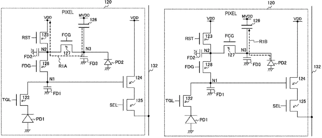
Sony has filed a patent for an imaging device that improves image quality by managing how electrical charge is stored in camera sensors. The design uses specific switches to reset a capacitor between reading image data and capturing the next frame, which helps prevent a known electrical effect from distorting the picture.
In the filing’s own words
To suppress deterioration in image quality due to dielectric absorption of a capacitor used for a charge accumulation unit. An imaging device includes: a photoelectric conversion unit; a capacitor having one end connected to the photoelectric conversion unit; a first transistor having one end connected to the capacitor and the other end connected to a first node; a second transistor having one end connected to the first node and the other end connected to a power supply; and a control unit that controls driving of the first transistor and the second transistor. The control unit turns on the first transistor and the second transistor in at least a part of a period from a read operation of reading a pixel voltage of the first node to a shutter operation of the photoelectric conversion unit.
What exactly they claim (claim 1)
1. An imaging device comprising: a photoelectric conversion unit; a capacitor having one end connected to the photoelectric conversion unit; a first transistor having one end connected to the capacitor and the other end connected to a first node; a second transistor having one end connected to the first node and the other end connected to a power supply; and a control unit that controls driving of the first transistor and the second transistor, wherein the control unit turns on the first transistor and the second transistor in at least a part of a period from a read operation of reading a pixel voltage of the first node to a shutter operation of the photoelectric conversion unit.
Facts
- Company
- Sony (SONY SEMICONDUCTOR SOLUTIONS CORPORATION)
- Official title
- IMAGING DEVICE
- Publication number
- US20260323176A1
- Application number
- 19486147
- Filed
- Dec 19, 2023
- Published
- Oct 15, 2026
- Inventors
- 2
- Claims
- 17
Classified under
H04N 25/585 Electricity & electronicsH04N 25/771 Electricity & electronicsH04N 25/78 Electricity & electronicsMore from Sony in Cameras & imaging
- Sony patents camera chips that sign photos to prove they are real Sep 15, 2026
- Sony patents camera setup that learns to mimic a virtual view Sep 1, 2026
- Sony patents camera method to reduce lag in burst mode photos Sep 1, 2026
- Sony patents camera sensor design to improve global shutter image quality Sep 1, 2026
- Sony patents camera lens that subtracts light waves to cut data processing Sep 8, 2026
Summaries are simplified from the filing’s own abstract and first claim. A patent filing is not a product announcement.
Patent data and drawings: U.S. Patent and Trademark Office (USPTO). Nebula is not affiliated with or endorsed by the USPTO.