Sony patents camera sensor design to keep light detection stable
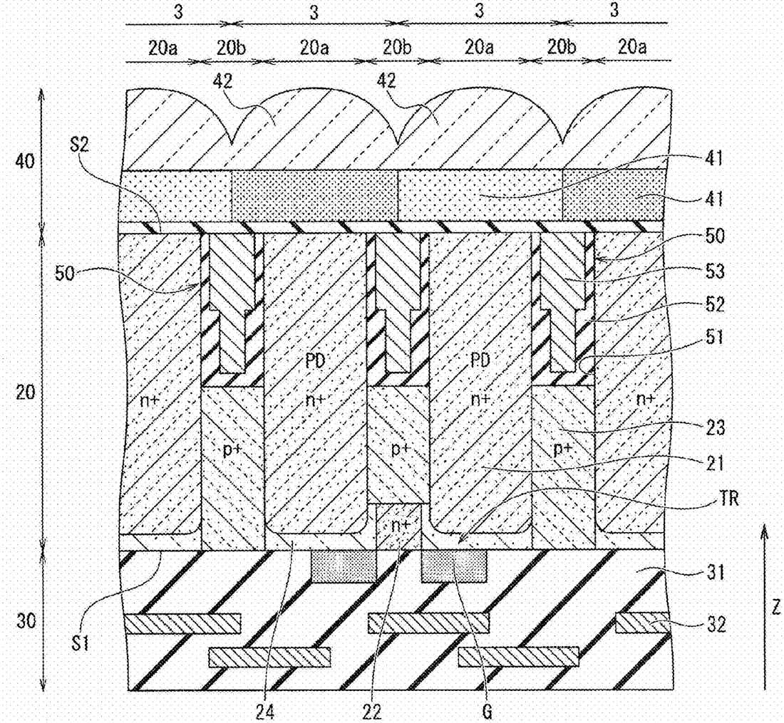
Sony describes a light detection device, likely for camera sensors, that uses a specific structure to separate individual pixels. The design features a conductive wall between pixels covered by an insulating film that is thinner on the side where light enters. This variation in thickness is intended to prevent the signal from degrading as it moves through the device.
In the filing’s own words
Provided is a light detection device capable of suppressing degradation of signal charge transfer characteristics. The light detection device includes: a semiconductor layer with one surface serving as an element formation surface and the other surface serving as a light incident surface, the semiconductor layer having a plurality of cell regions arranged in a matrix along row and column directions as viewed from above; a photoelectric conversion unit configured in each of the cell regions; and a trench isolation structure that extends along a thickness direction of the semiconductor layer and serves as a partition between the cell regions, the trench isolation structure includes a conductive wall including a conductive material, and an isolation insulating film that is provided on a side surface of the conductive wall and insulates the conductive wall from the semiconductor layer, and a film thickness of a portion of the isolation insulating film near the light incident surface is less than a film thickness of a portion near the element formation surface.
What exactly they claim (claim 1)
1. A light detection device comprising: a semiconductor layer with one surface serving as an element formation surface and an other surface serving as a light incident surface, the semiconductor layer having a plurality of cell regions arranged in a matrix along row and column directions as viewed from above; a photoelectric conversion unit configured in each of the cell regions; and a trench isolation structure that extends along a thickness direction of the semiconductor layer and serves as a partition between the cell regions, wherein the trench isolation structure includes a conductive wall including a conductive material, and an isolation insulating film that is provided on a side surface of the conductive wall and insulates the conductive wall from the semiconductor layer, and a film thickness of a portion of the isolation insulating film near the light incident surface is less than a film thickness of a portion near the element formation surface.
Facts
- Company
- Sony (SONY SEMICONDUCTOR SOLUTIONS CORPORATION)
- Official title
- LIGHT DETECTION DEVICE AND ELECTRONIC APPARATUS
- Publication number
- US20260314099A1
- Application number
- 19479540
- Filed
- Apr 18, 2024
- Published
- Oct 8, 2026
- Inventors
- 1
- Claims
- 11
Classified under
H10F 39/807 Electricity & electronicsMore from Sony in Cameras & imaging
- Sony patents camera chips that sign photos to prove they are real Sep 15, 2026
- Sony patents camera setup that learns to mimic a virtual view Sep 1, 2026
- Sony patents camera method to reduce lag in burst mode photos Sep 1, 2026
- Sony patents camera sensor design to improve global shutter image quality Sep 1, 2026
- Sony patents camera lens that subtracts light waves to cut data processing Sep 8, 2026
Summaries are simplified from the filing’s own abstract and first claim. A patent filing is not a product announcement.
Patent data and drawings: U.S. Patent and Trademark Office (USPTO). Nebula is not affiliated with or endorsed by the USPTO.