Sony patents camera sensor design with air gaps to improve image quality
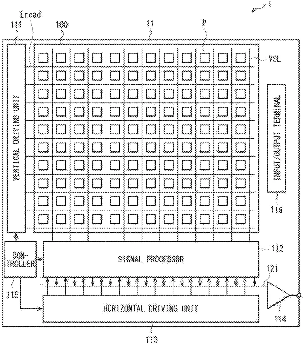
Sony has filed a patent for an imaging device that uses a specific arrangement of layers in camera pixels. The design includes an air gap between color filters and a metal layer to help separate the light-sensing parts of the sensor.
In the filing’s own words
An imaging device according to an embodiment of the present disclosure includes a plurality of pixels including a photoelectric conversion unit that photoelectrically converts light, a color filter provided for each pixel, a separation unit provided between the adjacent photoelectric conversion units, a structure having an air gap provided between the adjacent color filters, and a metal compound layer provided on the photoelectric conversion unit between the color filter and the photoelectric conversion unit. The structure is provided from between the adjacent color filters to the metal compound layer and is coupled to the separation unit.
What exactly they claim (claim 1)
1. An imaging device, comprising: a plurality of pixels including a photoelectric conversion unit that photoelectrically converts light; a color filter provided for each of the pixels; a separation unit provided between the adjacent photoelectric conversion units; a structure having an air gap provided between the adjacent color filters; and a metal compound layer provided on the photoelectric conversion unit between the color filter and the photoelectric conversion unit, wherein the structure is provided from between the adjacent color filters to the metal compound layer and is coupled to the separation unit.
Facts
- Company
- Sony (SONY SEMICONDUCTOR SOLUTIONS CORPORATION)
- Official title
- IMAGING DEVICE
- Publication number
- US20260314094A1
- Application number
- 18998625
- Filed
- Jul 25, 2023
- Published
- Oct 8, 2026
- Inventors
- 3
- Claims
- 20
Classified under
H10F 39/8053 Electricity & electronicsH10F 39/024 Electricity & electronicsH10F 39/182 Electricity & electronicsH10F 39/807 Electricity & electronicsMore from Sony in Cameras & imaging
- Sony patents camera chips that sign photos to prove they are real Sep 15, 2026
- Sony patents camera setup that learns to mimic a virtual view Sep 1, 2026
- Sony patents camera method to reduce lag in burst mode photos Sep 1, 2026
- Sony patents camera sensor design to improve global shutter image quality Sep 1, 2026
- Sony patents camera lens that subtracts light waves to cut data processing Sep 8, 2026
Summaries are simplified from the filing’s own abstract and first claim. A patent filing is not a product announcement.
Patent data and drawings: U.S. Patent and Trademark Office (USPTO). Nebula is not affiliated with or endorsed by the USPTO.