Samsung patents tiny image sensor pixels using 3x3 light filters
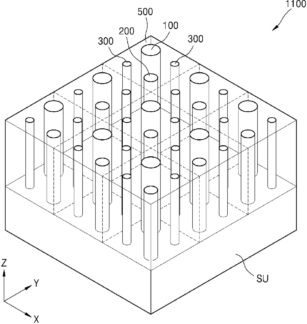
Samsung describes an image sensor where each pixel contains nine tiny light-absorbing elements arranged in a 3x3 grid. These elements are packed into an area smaller than 450 nanometers, which is below the physical limit where light usually spreads out. The design keeps the arrangement of these elements consistent across the center and edges of the sensor.
In the filing’s own words
An image sensor may include a pixel array including a plurality of two-dimensionally arranged pixels. Each pixel may include a first meta-photodiode absorbing light of a first wavelength band; a second meta-photodiode absorbing light in a second wavelength band; and a third meta-photodiode absorbing light of a third wavelength band, wherein the first meta-photodiode, the second meta-photodiode, and the third meta-photodiode may be arranged in an area having a size less than a diffraction limit. The arrangement form of the first meta-photodiode, the second meta-photodiode, and the third meta-photodiode arranged in the plurality of pixels in a central portion of the pixel array may be the same as the arrangement form of the first meta-photodiode, the second meta-photodiode, and the third meta-photodiode arranged in the plurality of pixels in a periphery of the pixel array.
What exactly they claim (claim 1)
1. An image sensor comprising: a pixel array comprising a plurality of two-dimensionally arranged pixels, wherein each of the plurality of pixels comprises: a first meta-photodiode configured to selectively absorb light of a first wavelength band; a second meta-photodiode configured to selectively absorb light of a second wavelength band different from the first wavelength band; and a third meta-photodiode configured to selectively absorb light of a third wavelength band different from the first wavelength band and second wavelength band, wherein, the first meta-photodiode, the second meta-photodiode, and the third meta-photodiode are arranged in an area having a size equal to or less than 450 nm×450 nm, wherein the first meta-photodiode, the second meta-photodiode, and the third meta-photodiode of one or more first pixels in a central portion of the pixel array, among the plurality of pixels, are arranged in a same form as the first meta-photodiode, the second meta-photodiode, and the third meta-photodiode of one or more second pixels in a periphery of the pixel array, among the plurality of pixels, wherein a sum of the number of the first meta-photodiodes, the second meta-photodiodes, and the third meta-photodiodes arranged in each of the plurality of pixels is nine, and the nine meta-photodiodes are arranged in the form of a 3×3 array.
Facts
- Company
- Samsung (SAMSUNG ELECTRONICS CO., LTD.)
- Official title
- IMAGE SENSOR AND ELECTRONIC APPARATUS INCLUDING THE IMAGE SENSOR
- Publication number
- US20260314087A1
- Application number
- 19711459
- Filed
- Jun 17, 2026
- Published
- Oct 8, 2026
- Inventors
- 4
- Claims
- 20
Classified under
H10F 39/182 Electricity & electronicsH10F 30/223 Electricity & electronicsH10F 39/806 Electricity & electronicsH10F 77/147 Electricity & electronicsMore from Samsung in Cameras & imaging
- Samsung patents syncing multiple cameras to record one video Sep 1, 2026
- Samsung patents camera system that auto-picks best lens for video Oct 13, 2026
- Samsung patents camera design that bends light to fit in thinner phones Oct 20, 2026
- Samsung patents camera feature that saves video clips around photos Sep 10, 2026
- Samsung patents image sensor that captures depth and bright scenes Sep 24, 2026
Summaries are simplified from the filing’s own abstract and first claim. A patent filing is not a product announcement.
Patent data and drawings: U.S. Patent and Trademark Office (USPTO). Nebula is not affiliated with or endorsed by the USPTO.