Sony patents lens coating method using separate chemical baths
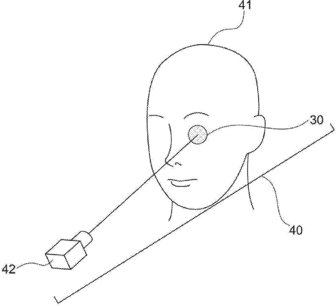
Sony describes a way to make optical elements by applying a light-sensitive layer and a protective layer to a base material. The process uses two different liquid solutions, where the second liquid does not dissolve the first layer, allowing them to be applied one after the other without mixing.
In the filing’s own words
A main object of the present technology is to provide a technology capable of suitably forming a photosensitive layer and a protective layer in relation to an optical element and a method for manufacturing the optical element. As a result of intensive studies, the present inventors have found that it is possible to form a photosensitive layer by using a photosensitive layer-forming solution prepared by dissolving a photosensitizing substance and a photosensitizing polymerizable monomer in a polar solvent, and to form a protective layer adjacent to the photosensitive layer by using a protective layer-forming solution, in which a protective polymer soluble in a protective layer solvent that does not dissolve the photosensitive layer is dissolved in the protective layer solvent, thereby suitably forming the photosensitive layer and the protective layer.
What exactly they claim (claim 1)
1. An optical element comprising: a base material layer; and at least a photosensitive layer and a protective layer adjacent to the photosensitive layer on one surface of the base material layer, wherein the photosensitive layer at least contains a derivative of a photosensitizing substance and a polymer of a photosensitizing polymerizable monomer, the protective layer contains a protective polymer soluble in a protective layer solvent and a compound related to the protective layer solvent, and the protective layer solvent does not dissolve the photosensitive layer.
Facts
- Company
- Sony (SONY GROUP CORPORATION)
- Official title
- OPTICAL ELEMENT, METHOD FOR MANUFACTURING OPTICAL ELEMENT, MATERIAL SET, OPTICAL DEVICE, AND SYSTEM
- Publication number
- US20260299167A1
- Application number
- 19478286
- Filed
- Apr 26, 2024
- Published
- Oct 1, 2026
- Inventors
- 5
- Claims
- 24
Classified under
G02B 1/043 Physics & computingB29D 11/00048 Operations & transportG02B 1/14 Physics & computingG02B 5/32 Physics & computingMore from Sony in Cameras & imaging
- Sony patents camera chips that sign photos to prove they are real Sep 15, 2026
- Sony patents camera setup that learns to mimic a virtual view Sep 1, 2026
- Sony patents camera method to reduce lag in burst mode photos Sep 1, 2026
- Sony patents camera sensor design to improve global shutter image quality Sep 1, 2026
- Sony patents camera lens that subtracts light waves to cut data processing Sep 8, 2026
Summaries are simplified from the filing’s own abstract and first claim. A patent filing is not a product announcement.
Patent data and drawings: U.S. Patent and Trademark Office (USPTO). Nebula is not affiliated with or endorsed by the USPTO.