Sony patents dual-camera system that saves power by skipping pixels
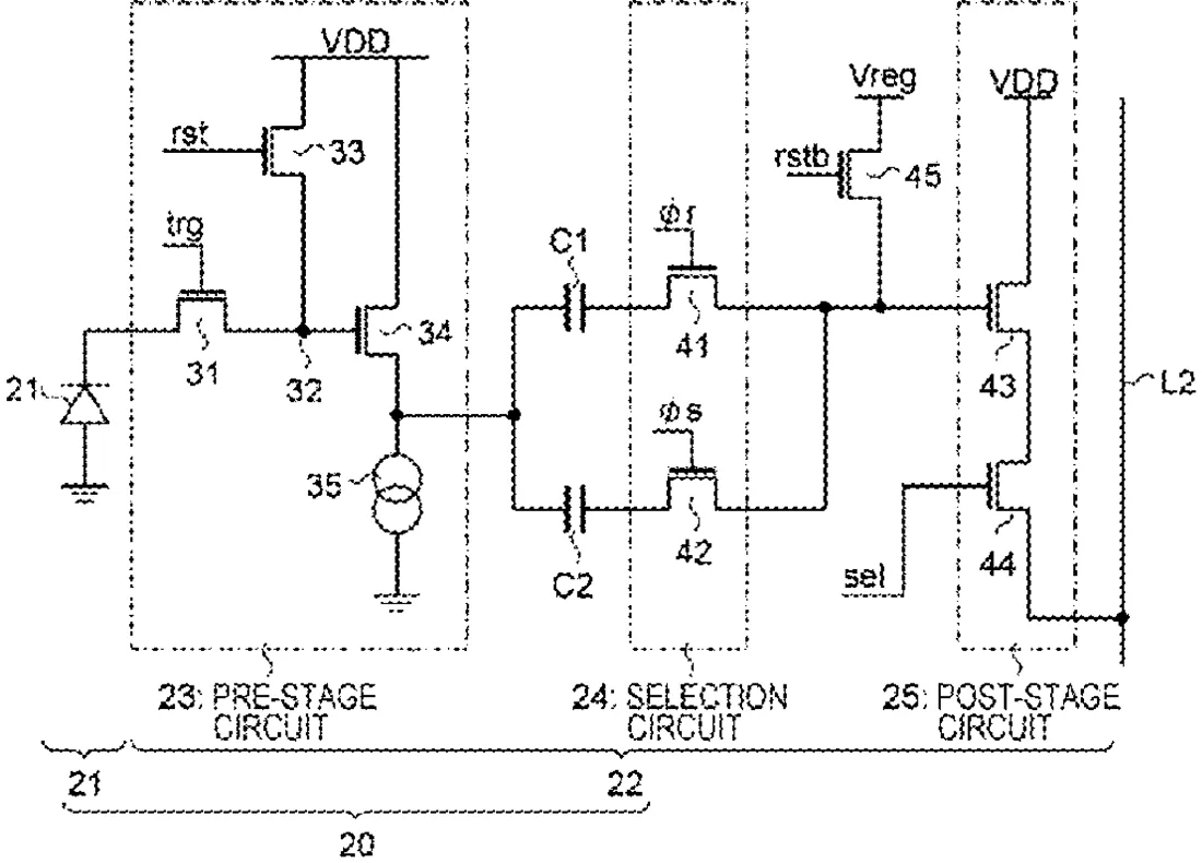
Sony has been granted a patent for a camera system using two image sensors that work together to reduce energy use. The system reads light data from pixels without destroying the stored charge, allowing the camera to decide which pixels to fully process based on the initial readings from either sensor.
In the filing’s own words
Camera imaging elements with reduced power consumption are disclosed. In one example, a first imaging element of a camera system includes first pixel circuits that simultaneously sample and non-destructively read charges according to incident light photoelectrically converted in each pixel. A second imaging element includes second pixel circuits that simultaneously sample and non-destructively read charges according to incident light photoelectrically converted in each pixel. The first imaging element selectively outputs a pixel signal from at least some of the first pixel circuits within a frame period on the basis of a pixel signal output from some of the first pixel circuits or the second pixel circuits, and the second imaging element selectively outputs a pixel signal from at least some of the second pixel circuits within the frame period on the basis of a pixel signal output from some of the first pixel circuits or the second pixel circuits.
What exactly they claim (claim 1)
1. A camera system comprising: a first imaging element; a second imaging element; and a control section that controls the first imaging element and the second imaging element, wherein the first imaging element includes a plurality of first pixel circuits that simultaneously samples charges according to incident light photoelectrically converted in each pixel and reads out the charges sampled in a non-destructive manner, the second imaging element includes a plurality of second pixel circuits that simultaneously samples charges according to incident light photoelectrically converted in each pixel and reads out the charges sampled in a non-destructive manner, the first imaging element switches whether or not to output a pixel signal from at least some first pixel circuits among the plurality of first pixel circuits within a same frame period on a basis of a pixel signal output from some of the first pixel circuits or some of the second pixel circuits for each frame period, and the second imaging element switches whether or not to output a pixel signal from at least some second pixel circuits among the plurality of second pixel circuits within a same frame period on a basis of a pixel signal output from the some first pixel circuits or the some second pixel circuits for each frame period.
Facts
- Company
- Sony (Sony Semiconductor Solutions Corporation)
- Official title
- Camera system and control method therefor
- Patent number
- US12771955B2
- Application number
- 18993968
- Filed
- Aug 16, 2023
- Granted
- Oct 20, 2026
- Inventors
- 1
- Claims
- 20
Classified under
H04N 23/90 Electricity & electronicsH04N 23/6811 Electricity & electronicsH04N 25/443 Electricity & electronicsH04N 25/78 Electricity & electronicsMore from Sony in Cameras & imaging
- Sony patents camera chips that sign photos to prove they are real Sep 15, 2026
- Sony patents camera setup that learns to mimic a virtual view Sep 1, 2026
- Sony patents camera method to reduce lag in burst mode photos Sep 1, 2026
- Sony patents camera sensor design to improve global shutter image quality Sep 1, 2026
- Sony patents camera lens that subtracts light waves to cut data processing Sep 8, 2026
Summaries are simplified from the filing’s own abstract and first claim. A patent filing is not a product announcement.
Patent data and drawings: U.S. Patent and Trademark Office (USPTO). Nebula is not affiliated with or endorsed by the USPTO.