Samsung patents camera sensor with variable nano-lenses
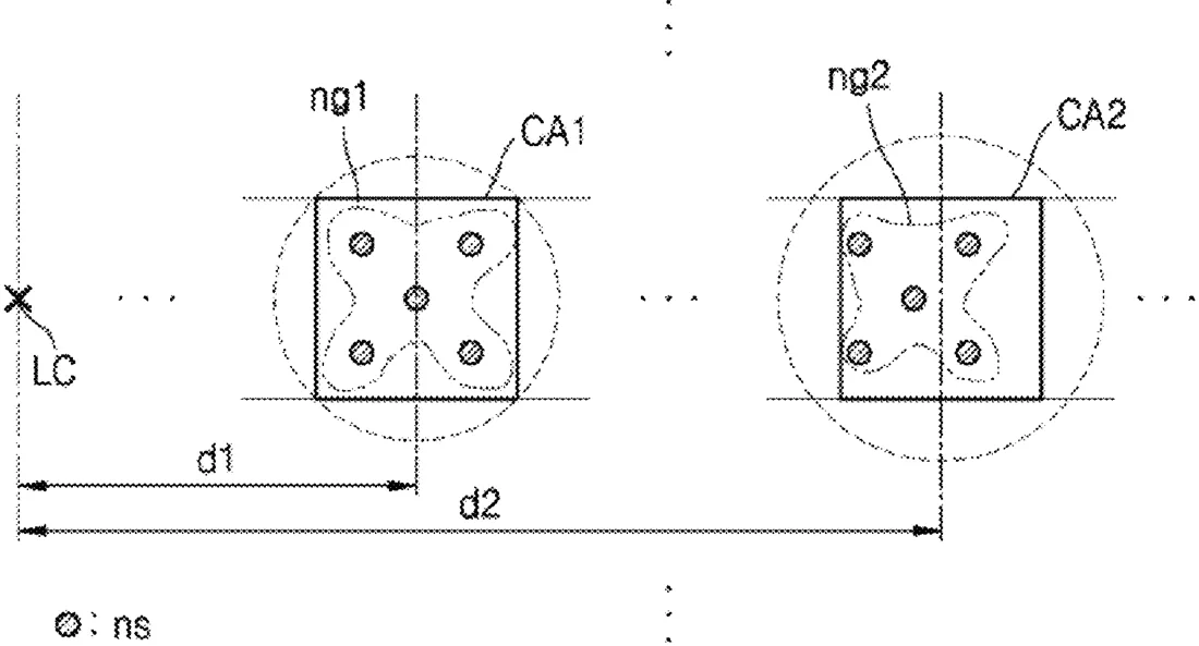
Samsung has been granted a patent for an image sensor that uses a layer of tiny nanostructures to focus light onto individual pixels. The design changes the focusing strength of these nanostructures based on their distance from the center of the sensor, allowing for more precise light collection across the entire image area.
In the filing’s own words
An image sensor including a pixel array in which a plurality of pixels are arranged, and a nano-condensing lens array including a plurality of condensing areas respectively corresponding to the plurality of pixels. Each of the plurality of condensing areas includes at least one nanostructure that condenses light on a corresponding pixel among the plurality of pixels, and the at least one nanostructure is arranged in each of the plurality of condensing areas such that a condensing capability of the at least one nanostructure included in each of the plurality of condensing areas varies according to a distance from a center of the nano-condensing lens array to each of the plurality of condensing areas.
What exactly they claim (claim 1)
1. An image sensor comprising: a pixel array including a plurality of pixels; and a nano-condensing lens array including a plurality of condensing areas respectively corresponding to the plurality of pixels, wherein each of the plurality of condensing areas comprises at least one nanostructure configured to condense light on a corresponding pixel from among the plurality of pixels, and the at least one nanostructure is arranged in each of the plurality of condensing areas such that a condensing capability of the at least one nanostructure included in each of the plurality of condensing areas is varied according to a distance from a center of the nano-condensing lens array to each of the plurality of condensing areas.
Facts
- Company
- Samsung (Samsung Electronics Co., Ltd.)
- Official title
- Imager with variable nanostructure
- Patent number
- US12765097B2
- Application number
- 18442612
- Filed
- Feb 15, 2024
- Granted
- Oct 13, 2026
- Inventors
- 5
- Claims
- 20
Classified under
H10F 39/8063 Electricity & electronicsG02B 3/0043 Physics & computingG02B 2207/101 Physics & computingMore from Samsung in Cameras & imaging
- Samsung patents syncing multiple cameras to record one video Sep 1, 2026
- Samsung patents camera system that auto-picks best lens for video Oct 13, 2026
- Samsung patents camera design that bends light to fit in thinner phones Oct 20, 2026
- Samsung patents camera feature that saves video clips around photos Sep 10, 2026
- Samsung patents image sensor that captures depth and bright scenes Sep 24, 2026
Summaries are simplified from the filing’s own abstract and first claim. A patent filing is not a product announcement.
Patent data and drawings: U.S. Patent and Trademark Office (USPTO). Nebula is not affiliated with or endorsed by the USPTO.