Sony patents camera sensor design with rounded edges for better image quality
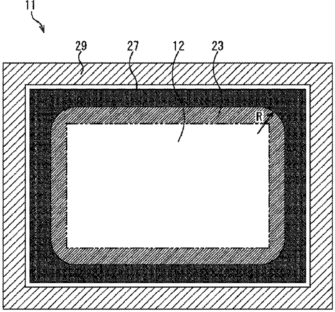
Sony describes a structure for camera sensors that places a special coating between the sensor chip and the protective glass frame. This coating reduces unwanted reflections and supports the glass while keeping the light-sensitive area clear.
In the filing’s own words
The present disclosure relates to an imaging element package and an electronic device that allow images to be captured with better quality. A support portion configured to support a cover glass that protects a light-receiving surface of a semiconductor substrate provided with a photodiode is provided along an outer periphery of the semiconductor substrate, and an antireflection layer is provided between the support portion and the semiconductor substrate at least in an area where the support portion is provided. The antireflection layer is provided entirely on the light-receiving surface of the semiconductor substrate, and the support portion is stacked on the antireflection layer. The present disclosure can be applied to a CMOS image sensor, for example.
What exactly they claim (claim 1)
1. An imaging element package, comprising: a semiconductor substrate provided with a photodiode; a support portion provided along an outer periphery of the semiconductor substrate to support a cover glass that protects a light-receiving surface of the semiconductor substrate; an antireflection layer provided between the support portion and the semiconductor substrate at least in an area where the support portion is provided; and a light-shielding layer provided stacked on the antireflection layer with a prescribed width outwardly from a boundary between an effective pixel area where pixels effectively used for capturing images are located and a peripheral area provided in a peripheral part outside of the effective pixel area, wherein the light-shielding layer has an outer shape having four corners rounded in an arc shape with a prescribed radius of curvature when viewed in a plan view, wherein the antireflection layer is provided entirely on the light-receiving surface of the semiconductor substrate, and wherein the support portion is stacked on the antireflection layer.
Facts
- Company
- Sony (SONY SEMICONDUCTOR SOLUTIONS CORPORATION)
- Official title
- Imaging element package and electronic device
- Patent number
- US12765094B2
- Application number
- 18566150
- Filed
- May 23, 2022
- Granted
- Oct 13, 2026
- Inventors
- 8
- Claims
- 18
Classified under
H10F 39/805 Electricity & electronicsH04N 25/79 Electricity & electronicsH10F 39/182 Electricity & electronicsH10F 39/804 Electricity & electronicsH10F 39/8057 Electricity & electronicsH10F 39/8063 Electricity & electronicsMore from Sony in Cameras & imaging
- Sony patents camera chips that sign photos to prove they are real Sep 15, 2026
- Sony patents camera setup that learns to mimic a virtual view Sep 1, 2026
- Sony patents camera method to reduce lag in burst mode photos Sep 1, 2026
- Sony patents camera sensor design to improve global shutter image quality Sep 1, 2026
- Sony patents camera lens that subtracts light waves to cut data processing Sep 8, 2026
Summaries are simplified from the filing’s own abstract and first claim. A patent filing is not a product announcement.
Patent data and drawings: U.S. Patent and Trademark Office (USPTO). Nebula is not affiliated with or endorsed by the USPTO.