Apple patents OLED screens with holes for better face sensors
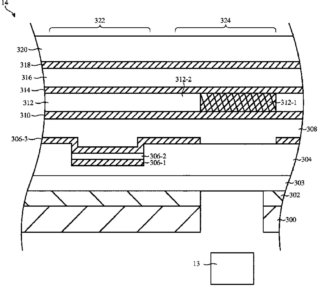
Apple describes a method for making OLED screens more transparent in specific areas to help sensors underneath see better. The design removes certain electronic components and layers from the screen in small regions directly above the sensor. This allows more light to pass through the display so the sensor can detect features like a user's face.
In the filing’s own words
An electronic device may include a display and an optical sensor formed underneath the display. A pixel removal region on the display may at least partially overlap with the sensor. The pixel removal region may include a plurality of non-pixel regions each of which is devoid of thin-film transistors. The plurality of non-pixel regions is configured to increase the transmittance of light through the display to the sensor. In addition to removing thin-film transistors in the pixel removal region, additional layers in the display stack-up may be removed. In particular, a cathode layer, polyimide layer, and/or substrate in the display stack-up may be patterned to have an opening in the pixel removal region. A polarizer may be bleached in the pixel removal region for additional transmittance gains. The cathode layer may be removed using laser ablation with a spot laser or blanket illumination.
What exactly they claim (claim 1)
1. An electronic device, comprising: a display that includes a plurality of pixels, at least one substrate, a thin-film transistor layer that is formed over the at least one substrate and that is configured to control the plurality of pixels, and an inorganic buffer layer interposed between the at least one substrate and the thin-film transistor layer, wherein the plurality of light-emitting diodes is formed on the thin-film transistor layer; and a sensor under the display, wherein the display comprises a pixel free region that at least partially overlaps with the sensor, wherein the at least one substrate has an opening in the pixel free region that increases the transmittance of light through the display to the sensor, wherein the thin-film transistor layer comprises a metal routing layer, wherein the thin-film transistor layer covers the opening, and wherein the inorganic buffer layer covers the opening.
Facts
- Company
- Apple (Apple Inc.)
- Official title
- Patterning in devices with organic light-emitting diode displays and sensors
- Patent number
- US12764213B2
- Application number
- 17802102
- Filed
- Feb 2, 2021
- Granted
- Oct 13, 2026
- Inventors
- 13
- Claims
- 21
Classified under
H04M 1/0266 Electricity & electronicsH10K 59/12 Electricity & electronicsH10K 59/122 Electricity & electronicsH10K 59/1201 Electricity & electronicsH10K 59/65 Electricity & electronicsH10K 59/80521 Electricity & electronicsMore from Apple in Phones & computers
- Apple patents foldable screen that warns you if you bend it too fast Sep 15, 2026
- Apple patents a button that senses pressure in three directions Oct 13, 2026
- Apple patents car key features inside its digital wallet app Sep 1, 2026
- Apple patents side button that vibrates sideways when pressed Sep 1, 2026
- Apple patents tablet cover that uses fabric to control folding angle Sep 15, 2026
Summaries are simplified from the filing’s own abstract and first claim. A patent filing is not a product announcement.
Patent data and drawings: U.S. Patent and Trademark Office (USPTO). Nebula is not affiliated with or endorsed by the USPTO.