Apple patents chip design that feeds power from the bottom of transistors
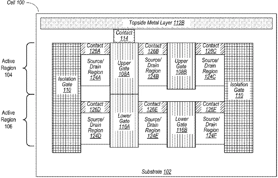
Apple describes a method for building computer chips where the power supply wires are located on the backside of the chip, while the signal wires stay on the top. This setup uses vertical transistors with a metal contact layer connecting the lower parts of the transistors to the backside power lines. The filing explains how these basic building blocks can be combined to create standard logic circuits like inverters and multiplexers.
In the filing’s own words
Various structures that implement topside metal routing and backside metal routing in combination with vertical transistors are disclosed. The various structures include a building block cell with a metal contact layer between the backside metal routing and the vertical transistors. Various connections can be made within the building block cell to form more complex structures such as, but not limited to, inverter devices, NAND devices, and MUX (multiplexer) devices.
What exactly they claim (claim 1)
1. An apparatus, comprising: a first vertical transistor formed in a transistor region of an integrated circuit cell structure, the first vertical transistor having a lower source/drain region, a first gate, and an upper source/drain region stacked in a vertical dimension; a second vertical transistor formed in the transistor region, the second vertical transistor having a lower source/drain region, a second gate, and an upper source/drain region stacked in the vertical dimension, wherein the second vertical transistor is parallel to the first vertical transistor with at least some spacing in a horizontal dimension between the first and second vertical transistors; a first metal layer located above the transistor region in the vertical dimension, wherein the first metal layer includes signal routing; a second metal layer located below the transistor region in the vertical dimension, wherein the second metal layer includes power routing; a third metal layer positioned below the lower source/drain regions and above the second metal layer, wherein the third metal layer includes at least one metal portion in contact with at least one of the lower source/drain regions; and a first via coupled between the at least one metal portion in the third metal layer and the power routing in the second metal layer.
Facts
- Company
- Apple (Apple Inc.)
- Official title
- Vertical transistors with backside power delivery
- Patent number
- US12757371B2
- Application number
- 18448715
- Filed
- Aug 11, 2023
- Granted
- Oct 6, 2026
- Inventors
- 3
- Claims
- 19
Classified under
H10B 10/125 Electricity & electronicsH10B 10/18 Electricity & electronicsH10D 30/63 Electricity & electronicsH10D 64/252 Electricity & electronicsH10D 64/518 Electricity & electronicsH10D 84/85 Electricity & electronicsMore from Apple in Chips & hardware
- Apple patents glass chip base that uses light to move data Oct 8, 2026
- Apple patents radar that maps rooms using moving objects Sep 1, 2026
- Apple patents display method that reuses static images to save power Sep 1, 2026
- Apple patents stretchable OLED displays with sealed pixel islands Sep 8, 2026
- Apple patents method to fix color fringes in high-resolution displays Sep 8, 2026
Summaries are simplified from the filing’s own abstract and first claim. A patent filing is not a product announcement.
Patent data and drawings: U.S. Patent and Trademark Office (USPTO). Nebula is not affiliated with or endorsed by the USPTO.