Apple patents display design that shrinks the border around camera holes
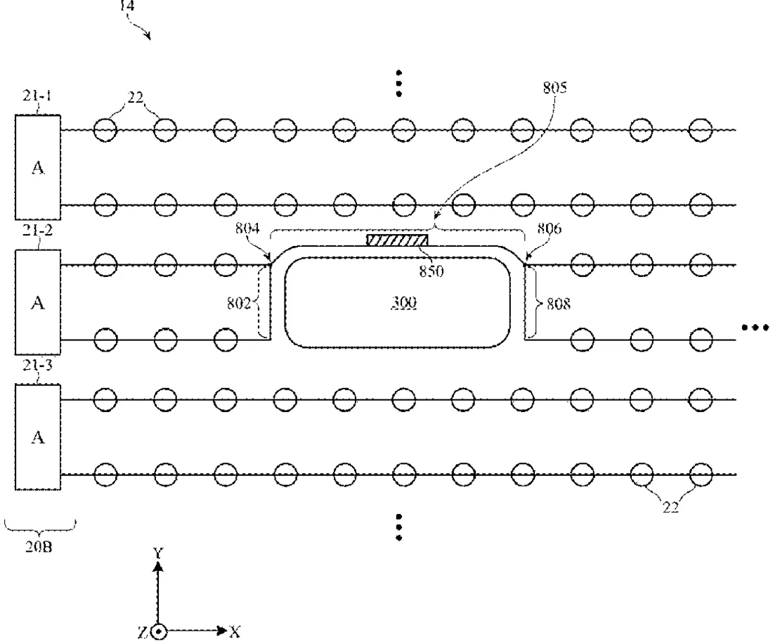
Apple describes a method for making screens with smaller, less noticeable cutouts for cameras or sensors. The design merges electrical wires before they route around the hole to reduce crowding and uses a tapered shape to maximize the usable screen area.
In the filing’s own words
An electronic device may include a display having display pixels formed in an active area of the display. The display further includes display driver circuitry for driving gate lines that are routed across the display. A hole such as a through hole, optical window, or other inactive region may be formed within the active area of the display. Multiple gate lines carrying the same signal may be merged together prior to being routed around the hole to help minimize the routing line congestion around the border of the hole. Dummy circuits may be coupled to the merged segment portion to help increase the parasitic loading on the merged segments. The hole may have a tapered shape to help maximize the size of the active area. The hole may have an asymmetric shape to accommodate multiple sub-display sensor components.
What exactly they claim (claim 1)
1. Display circuitry comprising: a substrate; an encapsulation layer over the substrate; thin-film transistor routing layers between the substrate and the encapsulation layer; first and second lines of display pixels formed in an active area and formed in the thin-film transistor routing layers; an inactive region within the active area and comprising an optical window formed from a portion of the substrate, formed between first and second opposing portions of the thin-film transistor routing layers, and formed from a portion of the encapsulation layer, wherein the portion of the substrate and the portion of the encapsulation layer is configured to pass optical signals; a first routing segment coupled to the first line of display pixels and formed in the first portion of the thin-film transistor routing layers; a second routing segment coupled to the second line of display pixels and formed in the first portion of the thin-film transistor routing layers; a merged segment into which the first and second routing segments are merged, wherein the merged segment is routed around the portion of the encapsulation layer forming the optical window from the first portion of the thin-film transistor routing layers to the second portion of the thin-film transistor routing layers and wherein the merged segment overlaps the active area; and display driver circuitry coupled to the first and second routing segments.
Facts
- Company
- Apple (Apple Inc.)
- Official title
- Reducing border width around a hole in display active area
- Patent number
- US12755688B2
- Application number
- 18449611
- Filed
- Aug 14, 2023
- Granted
- Oct 6, 2026
- Inventors
- 7
- Claims
- 20
Classified under
G09G 3/3225 Physics & computingG06F 3/0412 Physics & computingH10K 59/131 Electricity & electronicsH10K 59/65 Electricity & electronicsH10K 77/10 Electricity & electronicsMore from Apple in Phones & computers
- Apple patents foldable screen that warns you if you bend it too fast Sep 15, 2026
- Apple patents a button that senses pressure in three directions Oct 13, 2026
- Apple patents car key features inside its digital wallet app Sep 1, 2026
- Apple patents side button that vibrates sideways when pressed Sep 1, 2026
- Apple patents tablet cover that uses fabric to control folding angle Sep 15, 2026
Summaries are simplified from the filing’s own abstract and first claim. A patent filing is not a product announcement.
Patent data and drawings: U.S. Patent and Trademark Office (USPTO). Nebula is not affiliated with or endorsed by the USPTO.